Polarization field assisted heterostructure design for efficient deep ultra-violet light emitting diodes

a light-emitting diode and heterostructure technology, applied in the direction of basic electric elements, electrical equipment, semiconductor devices, etc., can solve the problems of low external quantum efficiency (eqe), poor doping efficiency, limited light extraction efficiency, etc., to minimize resistive losses and heat generation, reduce sheet resistance, and improve the effect of light extraction efficiency

Active Publication Date: 2021-03-23
CORNELL UNIVERSITY
View PDF5 Cites 0 Cited by
  • Summary
  • Abstract
  • Description
  • Claims
  • Application Information

AI Technical Summary

Benefits of technology

[0006]In one embodiment, the subject technology is a polarization field assisted DUV-LED comprising a bottom substrate, a n-contact / injection layer formed on the bottom substrate. The n-contact / injection layer includes: a first region for accommodating strain relaxation; a second region for lateral access with a low sheet resistance and higher conductivity compared to the first region to minimize resistive losses and heat generation; and a third region of a graded vertical injection layer with low vertical resistance to minimize heat loss due to vertical resistance. The DUV-LED also includes a p-contact region and an emitting active region between the n-contact / injection layer and the p-contact region. Preferably, the bottom substrate is Aluminum-Nitride (AlN) and the first region is a n-AlGaN region fabricated of a compositionally graded buffer region doped with n-type chemical impurity of a thickness in a range of 100-500 nanometer (nm). In the first region, an Aluminum content may be linearly graded down from a start value of 100% to an end value of 70% near the emitting active region. The second region may be a n-AlGaN region fabricated of a constant composition heavily impurity doped AlGaN lateral access region of a thickness greater than 1 micron. The third region can be a compositionally graded polarization doped AlGaN layer with n-type impurity having a thickness between about 100-200 nm.
[0008]In another embodiment, the subject technology is directed to a polarization field assisted DUV-LED including a bottom substrate, a n-contact / injection layer formed on the bottom substrate, a p-contact region, an emitting active region between the n-contact / injection layer and the p-contact region, a first metal contact attached to the first layer, a second metal contact attached to the contact region, a battery connected between the first and second metal contacts, and a monolithic FET switch connected in series with the battery for generating pulsed operation of the DUV-LED for thermal management. The n-contact / injection layer can includes a first region for accommodating strain relaxation. The n-contact / injection layer can also include a second region for lateral access with a low sheet resistance and higher conductivity compared to the first region to minimize resistive losses and heat generation. The n-contact / injection layer can also include a third region of a graded vertical injection layer with low vertical resistance to minimize heat loss due to vertical resistance.
[0009]Still another embodiment is a LED with enhanced EQE comprising compositionally graded AlGaN contact layers doped with chemical impurities for carrier injection from p and n regions to enhance a doping efficiency and thus improve injection efficiency. The contact layers can be formed by compositionally graded polarization-induced-doping. Preferably, the contact layers are field ionized and further comprising a p-contact layer including polarization field assisted tunnel junctions. A n-contact layer may include 3 distinct AlGaN regions of: a compositionally graded buffer region doped with n-type chemical impurity to accommodate strain relaxation; a constant composition heavily impurity doped thick AlGaN lateral access region; and a compositionally graded polarization doped layer with n-type impurity as a vertical injection layer. The LED may further include a deep-UV light emitting active region composed of ultra-thin GaN / AlN quantum structures with high internal quantum efficiency due to improved electron-hole overlap. The LED can include a deep-UV light emitting active region composed of ultra-thin GaN / AlN quantum structures with high light extraction efficiency due to TE dominated light emission toward top surface of LED device.

Problems solved by technology

DUV emission from LEDs using AlGaN multi-quantum well light-emitting active regions has been demonstrated but typically suffers from low external quantum efficiency (EQE), which drops particularly for wavelengths shorter than 240 nm.
Several factors contribute to the low EQE such as: growth of LED structures on non-native substrates create large lattice mismatch, leading to dislocation densities; poor doping efficiency; limited light extraction efficiency because of total internal reflection due to refractive index mismatch; and polarization properties of the emitted light that makes light extraction efficiency difficult.
Low internal quantum efficiency (IQE) is also a barrier to product development.

Method used


Image

  • Polarization field assisted heterostructure design for efficient deep ultra-violet light emitting diodes
  • Polarization field assisted heterostructure design for efficient deep ultra-violet light emitting diodes
  • Polarization field assisted heterostructure design for efficient deep ultra-violet light emitting diodes

Examples


Embodiment Construction

[0014]The subject technology overcomes many of the prior art problems associated with DUV LEDs. The advantages, and other features of the technology disclosed herein, will become more readily apparent to those having ordinary skill in the art from the following detailed description of certain preferred embodiments taken in conjunction with the drawings which set forth representative embodiments of the present technology and wherein like reference numerals identify similar structural elements. Directional indications such as upward, downward, right, left, bottom, top and the like are used with respect to the figures and not meant in a limiting manner.

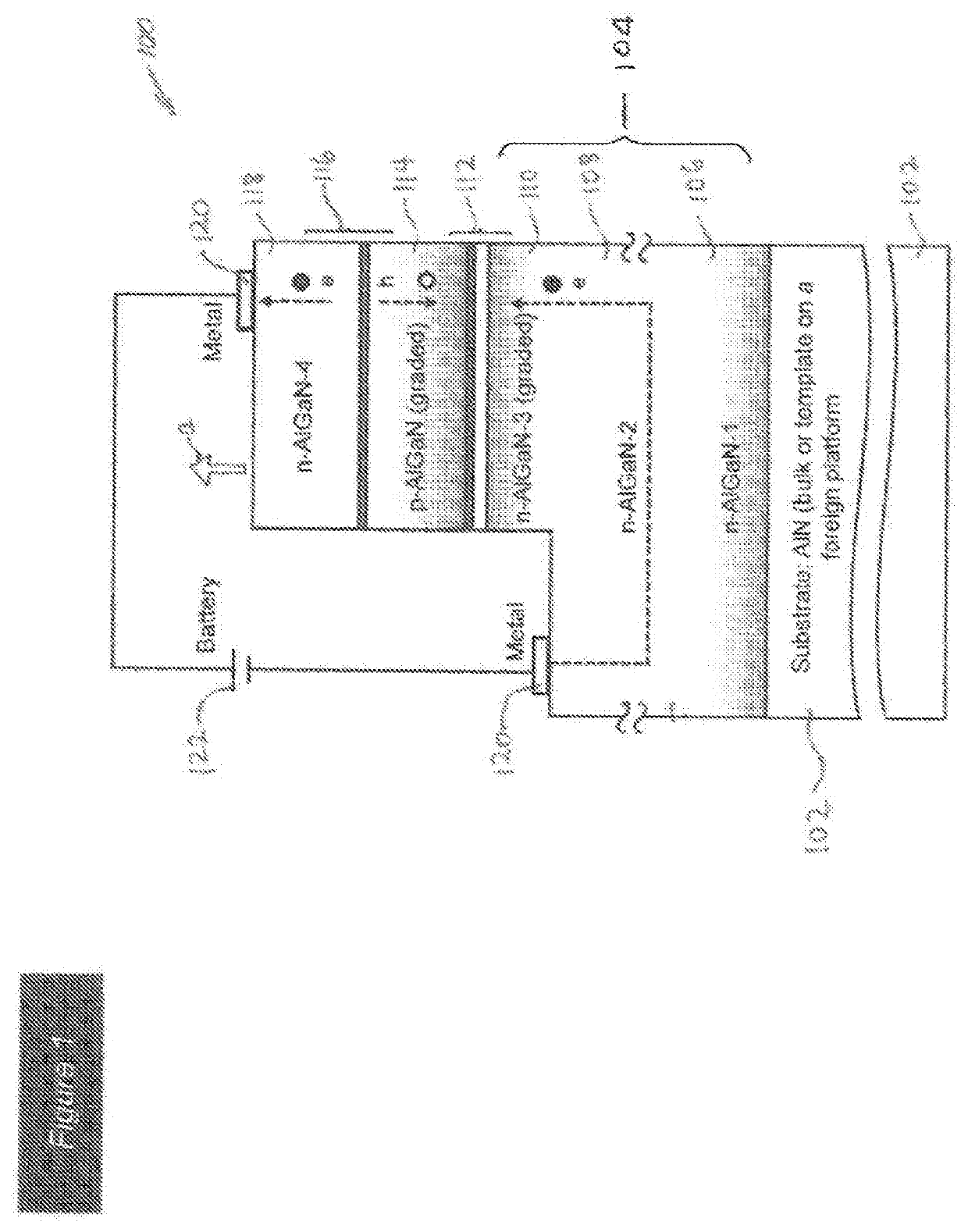
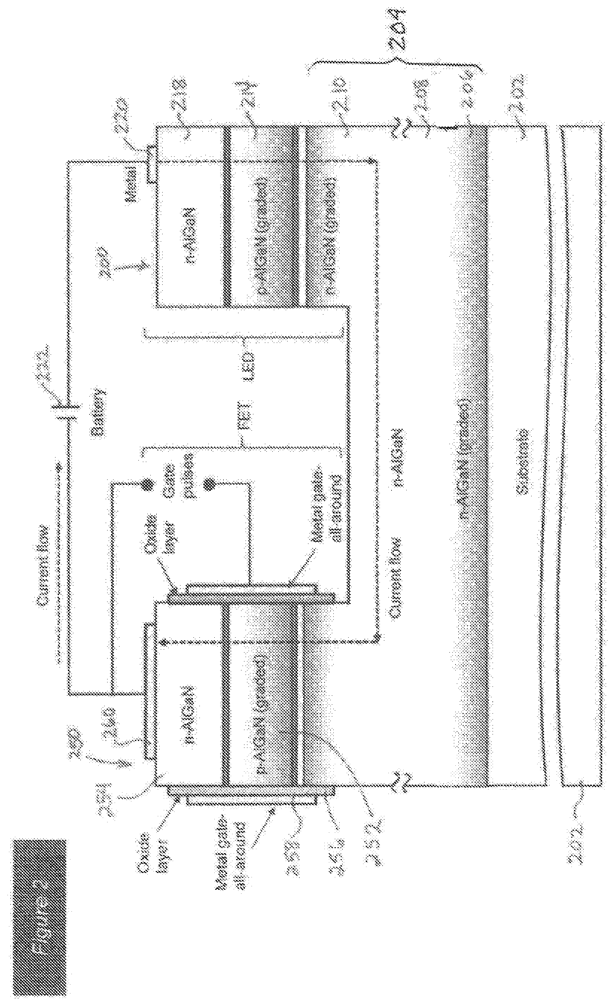
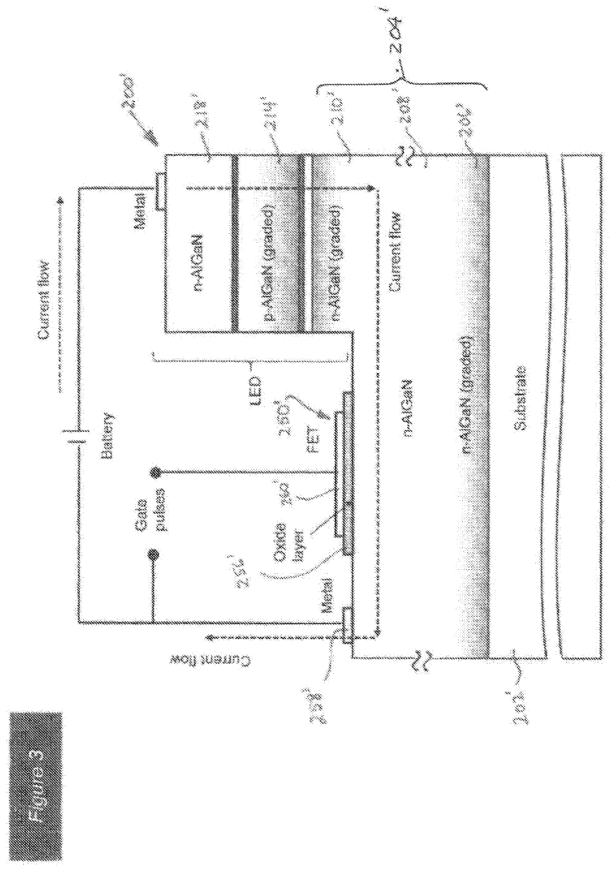
[0015]In brief overview, the subject technology realizes deep UV LEDs (DUV-LEDs) with design and crystal growth methods using molecular beam epitaxy (MBE). For example, the DUV-LED consists of a n-doped injection region, a p-doped injection region with polarization field-assisted doping with ternary AlGaN (Aluminum-Gallium-Nitride) wide ...


PUM

PropertyMeasurementUnit
thicknessaaaaaaaaaa
thicknessaaaaaaaaaa
thicknessaaaaaaaaaa

Abstract

A polarization field assisted DUV-LED including a bottom substrate and a n-contact / injection layer formed on the bottom substrate. The n-contact / injection layer includes: a first region for accommodating strain relaxation; a second region for lateral access with a low sheet resistance and higher conductivity compared to the first region to minimize resistive losses and heat generation; and a third region of a graded vertical injection layer with low vertical resistance to minimize heat loss due to vertical resistance. The DUV-LED also includes a p-contact region, and an emitting active region between the n-contact / injection layer and the p-contact region. The injection of electrons and holes into quantum wells proceeds due to tunneling of electrons and holes under the barriers due to less than 2 nm thickness of barriers. This carrier injection lowers the Turn ON voltage of LEDs and reduces heat generation.

Description

CROSS-REFERENCE TO RELATED APPLICATIONS[0001]This application claims priority to U.S. Provisional Patent Application No. 62 / 586,466, filed Nov. 15, 2017, and U.S. Provisional Patent Application No. 62 / 586,488, filed Nov. 15, 2017, each of which is incorporated herein by reference.BACKGROUND OF THE INVENTION1. Field of the Invention[0002]The subject disclosure relates to light-emitting diodes (LEDs), and more particularly to improved efficiency in LEDs.2. Background of the Related Art[0003]Replacing mercury-based DUV lamps with semiconductor LEDs is environmentally friendly, enables miniaturization, and enhances portability. DUV emission from LEDs using AlGaN multi-quantum well light-emitting active regions has been demonstrated but typically suffers from low external quantum efficiency (EQE), which drops particularly for wavelengths shorter than 240 nm. Several factors contribute to the low EQE such as: growth of LED structures on non-native substrates create large lattice mismatch,...

Claims


Application Information

Patent Timeline
Patent Type & Authority Patents(United States)
IPC IPC(8): H01L33/32H01L33/14H01L33/00H01L33/02H01L27/15H01L33/06H01L33/12H01L33/30H01L33/38
CPCH01L33/32H01L27/15H01L33/007H01L33/0025H01L33/0062H01L33/0075H01L33/02H01L33/025H01L33/06H01L33/12H01L33/14H01L33/30H01L33/325H01L33/38
Inventor ISLAM, SMPROTASENKO, VLADIMIRXING, HUILI GRACEJENA, DEBDEEP
Owner CORNELL UNIVERSITY
Why Eureka
Try Eureka