Atomic layer etching using acid halide

a technology of acid halide and atomic layer, applied in the direction of basic electric elements, electrical equipment, chemical instruments and processes, etc., can solve the problems of difficult adjustment of the thickness of the modified layer to the thickness of a single atomic layer, high accuracy required in each step of etching, etc., to achieve easy control of the etching amount and improve controllability and reproducibility.

Active Publication Date: 2021-11-23
KANTO DENKA IND CO LTD
View PDF12 Cites 0 Cited by
  • Summary
  • Abstract
  • Description
  • Claims
  • Application Information

AI Technical Summary

Benefits of technology

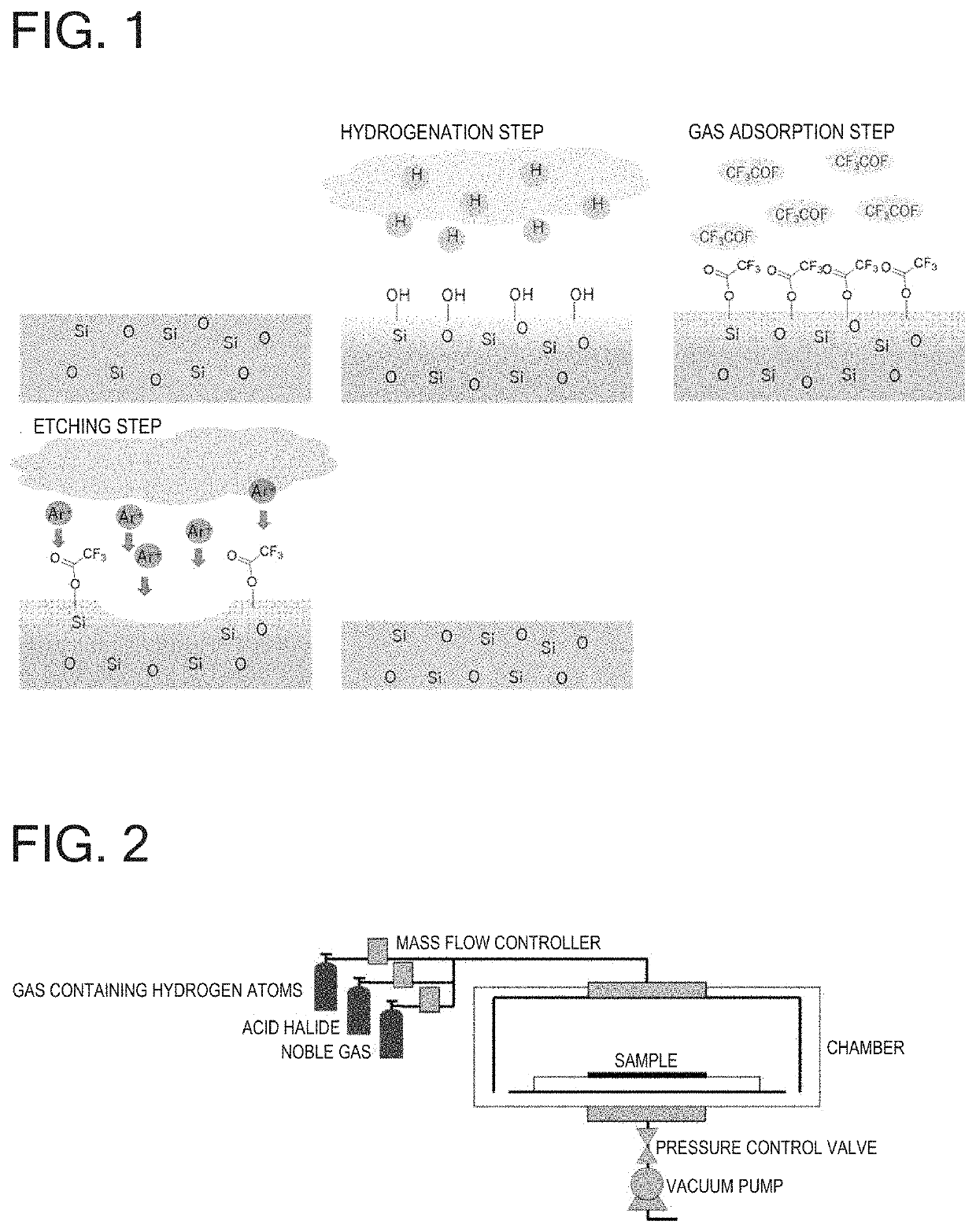
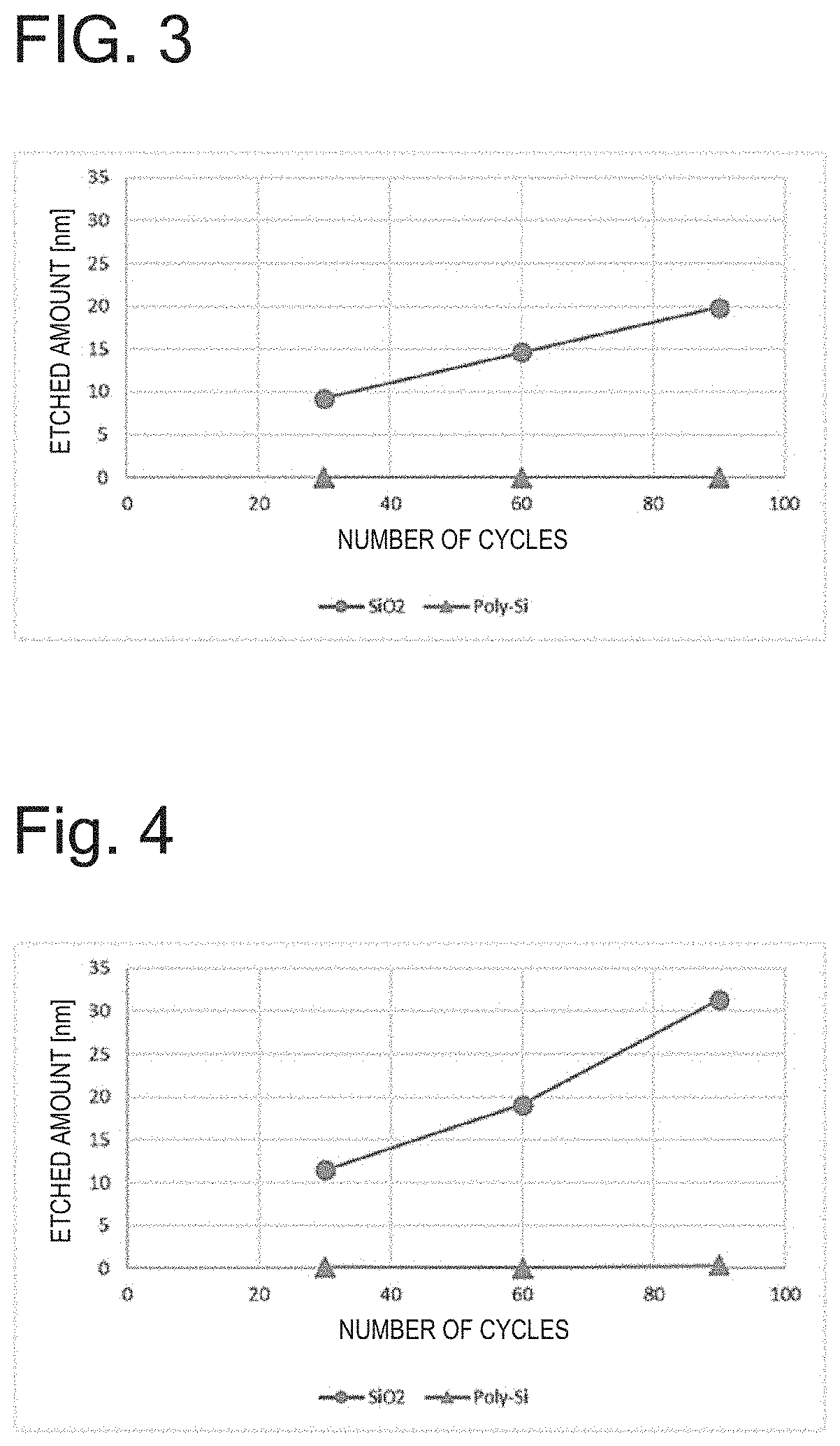
[0036]The present invention overcomes problems of the conventional methods of atomic layer etching for an etching target composed of a plurality of elements and provides a method of atomic layer etching with better controllability and reproducibility. First, the mechanism of atomic layer etching in the present invention will be described with reference to FIG. 1, which is an exemplary case of etching SiO2 by using H2 as a gas containing hydrogen, CF3COF as an acid halide, and Ar as a noble gas.
[0037]First, when the SiO2 surface is treated with H2 plasma, Si—OH is formed near the surface through, for example, collision of H+ ions with the SiO2 surface or adsorption of H radicals on the SiO2 surface. Upon exposure to CF3COF, CF3COF and Si—OH are reacted on the outermost surface while chemisorbing CF3COF as Si—O—COCF3 on the surface and releasing HF. Upon irradiation with Ar plasma, Ar+ ions collide with the SiO2 surface where CF3COF has been chemisorbed, thereby exciting chemical reactions in CF3COF-chemisorbed portions and desorbing volatile SiFx, COx, and / or CFx from the SiO2 surface. Consequently, etching progresses.
[0038]The present invention that performs atomic layer etching through the above-described mechanism exerts the following advantageous effects.
[0039](1) An acid halide is chemisorbed on the surface of an etching target by reactions between the acid halide and hydrogen atom-terminated substituents, such as hydroxyl groups and amino groups, formed on the outermost surface of the etching target through treatment with a plasma containing hydrogen. Hence, when the hydrogen-terminated substituents are consumed by the reactions, adsorption of the acid halide ceases. Accordingly, supply of elements required for etching is always stable, and consequently, fine tuning of duration of gas supply is not needed and the etched amount is easily controlled.(2) Even when hydrogen termination is performed through plasma treatment, but when generated substituents do not react with an acid halide (for example, C—H), an acid halide is not adsorbed on the surface of such a substance. Different from an etching target on which an acid halide is adsorbed, etching of such a substance is unlikely to progress in the etching step. Accordingly, it is possible to perform atomic layer etching of an etching target with high selectivity to such a substance.(3) The amount of an acid halide adsorbed on the inner wall of an apparatus that performs atomic layer etching, as that on an etching target, does not increase further once substituents that react with the acid halide are consumed. Hence, different from the case that uses a fluorocarbon gas as in the preceding inventions, there is no risk of deposition as a film or the resulting excessive supply of elements that contribute to etching. Moreover, surface contamination by particles due to peeling of a film per se does not occur. Accordingly, etching with good controllability and high reproducibility is possible even when the number of atomic layer etching repeated is increased.(4) The reactions between the surface of a hydrogen-terminated etching target and an acid halide progress at normal temperature. In addition, the subsequent induction of etching reactions is performed by irradiation with a plasma of a noble gas. Accordingly, heating of an etching target is not required, and consequently, atomic layer etching is possible while suppressing thermal deformation and / or stress damages therefrom.(5) An acid halide used in the present invention is composed of C, H, O, and X (X is any of F, Cl, Br, and I). These elements tend to form volatile compounds and are less likely to remain on a processed substrate after atomic layer etching as well. Accordingly, atomic layer etching is possible without contamination on a processed substrate or deterioration of physical properties of a substance on the substrate after etching.(6) Atomic layer etching of the present invention is not a method in which elements that contribute to etching are supplied in a form of a deposition film as in the preceding inventions. Accordingly, even when atomic layer etching is performed for patterns, such as line & space as well as holes, there is neither film deposition on pattern sidewalls nor risk of blocking of pattern openings. Hence, atomic layer etching of the present invention is applicable even to high-aspect-ratio patterns.

Problems solved by technology

Accordingly, extremely high accuracy is required in each step of etching, film forming, and the like, and conventional etching techniques and film forming techniques have already faced difficulties in handling such a requirement.
Compared with ALD, adjusting the thickness of the modified layer to the thickness of a single atomic layer is difficult in ALE.
When etching progresses more than necessary or when the thickness of the modified layer is uneven, there is a problem in which etching with high in-plane uniformity becomes difficult.
Accordingly, it is generally difficult to etch with good controllability of the thickness at a single atomic layer level.
Taking into account the fact that the actual thickness of a single atomic layer of SiO2 is about 0.18 nm, etching with good controllability of a single atomic layer is considered to be unsuccessful.
Moreover, there is a risk of making precise control difficult depending on an apparatus used due to the extremely short duration of gas supply and / or RF power application.
In addition, deposition of a fluorocarbon film on the chamber wall, through accumulation, involves a risk of contamination of a wafer as particles.
Although the number of cycles needs to be increased in ALE when the etched amount is large, such a measure is considered to be difficult to adopt in the method of NPL 1.
Moreover, from the nature of the reaction cycle employed, Al, C, H, F, and the like eventually remain on the SiO2 film surface, and hence, electrical characteristics of SiO2 could possibly deteriorate.

Method used


Image

  • Atomic layer etching using acid halide
  • Atomic layer etching using acid halide
  • Atomic layer etching using acid halide

Examples


example 1

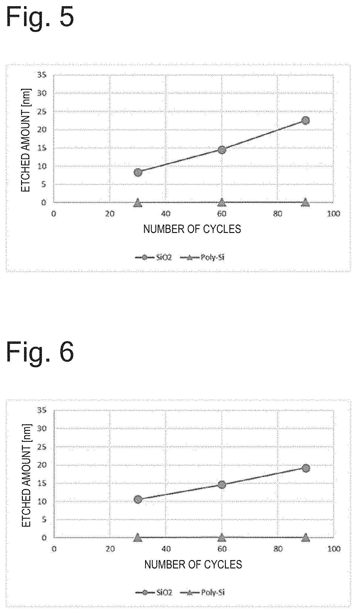
[0067]In accordance with the conditions of Table 1, a SiO2 sample (SiO2: 1,000 nm on Si substrate) and polysilicon (Poly-Si) samples (Poly-Si: 300 nm on SiO2 substrate; 100 nm on Si substrate) were subjected to 30 cycles of etching while using H2 as a gas containing hydrogen atoms in the hydrogenation step, CF3COF as an acid halide in the acid halide adsorption step, and using Ar as a noble gas and setting RF power to 60 W in the etching step. One cycle progresses in the order of (1)→(2)→(3)→(4)→(5)→(6) of Table 1, and processing is started from (1) again in the next cycle. As a result, the etched amount of SiO2 was 9.3 nm (0.31 nm / cycle) and the etched amount of Poly-Si was 0.0 nm (0.0 nm / cycle).

[0068]Next, when the same samples were subjected to 60 cycles of etching under the same conditions, the etched amount of SiO2 was 14.6 nm (0.24 nm / cycle) and the etched amount of Poly-Si was 0.0 nm (0.0 nm / cycle).

[0069]Further, after 90 cycles of etching, the etched amount of SiO2 was 19.9 ...

example 2

[0071]In accordance with the conditions of Table 1, a SiO2 sample (SiO2: 1,000 nm on Si substrate) and Poly-Si samples (Poly-Si: 300 nm on SiO2 substrate; 100 nm on Si substrate) were subjected to 30 cycles of etching while using H2 as a gas containing hydrogen atoms in the hydrogenation step, CHF2COF as an acid halide in the acid halide adsorption step, and using Ar as a noble gas and setting RF power to 60 W in the etching step. As a result, the etched amount of SiO2 was 11.5 nm (0.38 nm / cycle) and the etched amount of Poly-Si was 0.2 nm (0.007 nm / cycle).

[0072]Next, when the same samples were subjected to 60 cycles of etching under the same conditions, the etched amount of SiO2 was 19.1 nm (0.32 nm / cycle) and the etched amount of Poly-Si was 0.1 nm (0.002 nm / cycle).

[0073]Further, after 90 cycles of etching, the etched amount of SiO2 was 31.4 nm (0.35 nm / cycle) and the etched amount of Poly-Si was 0.4 nm (0.004 nm / cycle).

[0074]The above results are summarized in FIG. 4.

example 3

[0075]In accordance with the conditions of Table 1, a SiO2 sample (SiO2: 1,000 nm on Si substrate) and Poly-Si samples (Poly-Si: 300 nm on SiO2 substrate; 100 nm on Si substrate) were subjected to 30 cycles of etching while using H2 as a gas containing hydrogen atoms in the hydrogenation step, CF3COF as an acid halide in the acid halide adsorption step, and using Ar as a noble gas and setting RF power to 30 W in the etching step. As a result, the etched amount of SiO2 was 8.4 nm (0.28 nm / cycle) and the etched amount of Poly-Si was 0.0 nm (0 nm / cycle).

[0076]Next, when the same samples were subjected to 60 cycles of etching under the same conditions, the etched amount of SiO2 was 14.6 nm (0.24 nm / cycle) and the etched amount of Poly-Si was 0.0 nm (0 nm / cycle).

[0077]Further, after 90 cycles of etching, the etched amount of SiO2 was 22.6 nm (0.25 nm / cycle) and the etched amount of Poly-Si was 0.1 nm (0.001 nm / cycle).

[0078]The above results are summarized in FIG. 5.


PUM


Abstract

A method of atomic layer etching a silicon oxide film or a silicon nitride film is provided. Atomic layer etching (ALE) is performed by repeating three steps of (1) hydrogenation step of hydrogenating a surface by irradiating a silicon oxide film or a silicon nitride film with a plasma containing H, (2) acid halide adsorption step of causing chemisorption of an acid halide represented by a formula of Rf—COX (Rf is H, F, a substituent consisting of C and F or consisting of C, H, and F, or —COX; each X is independently any halogen atom of F, Cl, Br and I) on the surface by reacting the acid halide with the hydrogenated surface through exposure to the acid halide, and (3) etching step of etching a single atomic layer by inducing chemical reactions on the surface of the acid halide-adsorbed silicon oxide film or silicon nitride film through irradiation with a plasma containing a noble gas (at least any one of He, Ar, Ne, Kr, and Xe).

Description

TECHNICAL FIELD[0001]The present invention relates to atomic layer etching (ALE) for etching the thickness of a single atomic layer by: hydrogenating a surface of an etching target; causing chemisorption of an acid halide represented by Rf—COX (Rf is H, F, a substituent consisting of C and F, a substituent consisting of C, H, and F, or —COX; each X is independently any halogen atom of F, Cl, Br, and I) on the hydrogenated etching target through exposure to the acid halide; and etching the surface of the acid halide-adsorbed etching target through irradiation with a plasma containing a noble gas.BACKGROUND ART[0002]Leading-edge semiconductor devices are undergoing further high integration still today through microfabrication and adoption of three-dimensional structures, for example.[0003]In logic devices, miniaturization has progressed to the extent that a gate length and a half-pitch of flash memory reach a single-digit nm level. Accordingly, extremely high accuracy is required in e...

Claims


Application Information

Patent Timeline
Patent Type & Authority Patents(United States)
IPC IPC(8): H01L21/311
CPCH01L21/31116H01L21/3065H01L21/02131C09K13/00
Inventor KATO, KOREHITOFUKAE, KATSUYATAKAHASHI, YOSHINAO
Owner KANTO DENKA IND CO LTD
Why Eureka
Try Eureka