Microwave plasma reactor for manufacturing synthetic diamond material

a plasma reactor and diamond technology, applied in the direction of crystal growth process, polycrystalline material growth, chemically reactive gas, etc., can solve the problems of limited area over which diamond film can be deposited, non-uniform diamond film formation, etc., and achieve high gas stream velocities

Active Publication Date: 2022-06-28
ELEMENT SIX TECH LTD
View PDF139 Cites 0 Cited by
  • Summary
  • Abstract
  • Description
  • Claims
  • Application Information

AI Technical Summary

Benefits of technology

[0023]The present inventors have found that in contrast to the teachings of US2010 / 0189924, it is advantageous to provide a gas inlet configuration in which gas inlets are not angled inwardly to interact above the substrate and constrain the plasma in a lateral direction. While the commercially available IPLAS reactor discloses such a non-angled gas inlet configuration, both the IPLAS reactor and the reactor disclosed in US2010 / 0189924 have a relatively small number of gas inlets. In contrast to both these arrangements, the present inventors have found that instead of providing a relatively small number of gas inlets, the problems of gas stream punch-through in a central region of the plasma discharge at very high gas stream velocities can be reduced by providing a higher number of gas inlets which are substantially parallel or divergent in orientation.
[0024]In addition, it has been found that the relatively high number of gas inlets should be closely spaced to ensure a relatively uniform flow of gas. It has been found that providing a relatively high number density of gas inlets in an array improves the uniformity of gas flow towards the substrate in use and allows the plasma to be uniformly flattened and shaped relative to the substrate to achieve uniform diamond film formation at high rates over a relatively large area.
[0025]It has also been found to be useful to provide relatively small area gas inlets such that the area of the gas inlet array is largely made up of the space in-between the gas inlets rather than the area of the outlets of the gas inlets. As such, whereas it has been found to be advantageous to provide a relatively large number density of gas inlets in relation to the area of the gas inlet inlet array, it has also been found to be advantageous to provide an array in which the ratio of the area of the gas inlets divided by the area of the gas inlet array as a whole is low. It has been found that small gas inlets are advantageous for providing high velocity directed gas flows. However, it is also desired to have a relatively uniform gas flow over a relatively large area for uniform deposition of a diamond film over a relatively large area. Accordingly, a combination of relatively small gas inlet size and a relatively high number density of such gas inlets has been found to be advantageous to achieve a balance between high velocity directed gas flows and uniformity of gas flow over a relatively large area.

Problems solved by technology

However, one problem with the single axially positioned gas inlet arrangement disclosed in EP0480581 is that at very high velocity flows, the gas stream can penetrate through the plasma, essentially punching a hole in the plasma discharge and pushing the plasma outwards towards the sides of the substrate, leading to non-uniform diamond film formation.
One problem is that if the gas streams are angled to laterally constrain the plasma discharge, this will limit the area over which a diamond film can be deposited.
Alternatively, if the gas streams are angled to push against a more central region of the plasma such that the outer portions of the plasma are not constrained, then this will actually exacerbate the problem of punch-through in a central region of the plasma, such that the plasma is pushed towards the sides of the substrate leading to non-uniform diamond film formation.
Another possible problem with the arrangement described in US2010 / 0189924 is that the plasma must be constrained in a lateral direction to ensure that it does not impinge upon the corner portions of the plasma reactor located between the central, vertically extended portion in which the inlet nozzles are provided and the laterally extending side portions of the plasma chamber.
If the plasma were to impinge on these portions of the wall of the plasma chamber, the wall may be damaged in these regions.
Furthermore, contamination by process gases may build up on the wall resulting in a degradation of the diamond film quality formed in the reactor over time.
Another possible problem with the arrangement described in US2010 / 0189924 is that the plasma must be constrained such that it does not ignite at high energy microwave anti-nodes disposed within the laterally extending side portions of the plasma chamber.
This would lead to a reduction in power efficiency and could also damage the wall of the plasma chamber and cause contamination to build up on the walls resulting in a degradation of the diamond film quality formed in the reactor over time.
Yet another possible problem with the arrangement described in US2010 / 0189924 is that the microwave window is positioned in a base of the plasma chamber down stream of the inlet nozzles.
This may lead to contamination of the microwave window with process gases or wall contaminants falling onto the window resulting in a reduction in performance, such as might be associated with increased microwave absorption at the window area.
Although the IPLAS reactor comprises parallel oriented gas inlets rather than gas inlets which are angled inwardly as in US2010 / 0189924, it has been found that the relatively small number of gas inlets provided by this arrangement is insufficient to provide uniform diamond film formation at high rates over a relatively large area.

Method used


Image

  • Microwave plasma reactor for manufacturing synthetic diamond material
  • Microwave plasma reactor for manufacturing synthetic diamond material
  • Microwave plasma reactor for manufacturing synthetic diamond material

Examples


Embodiment Construction

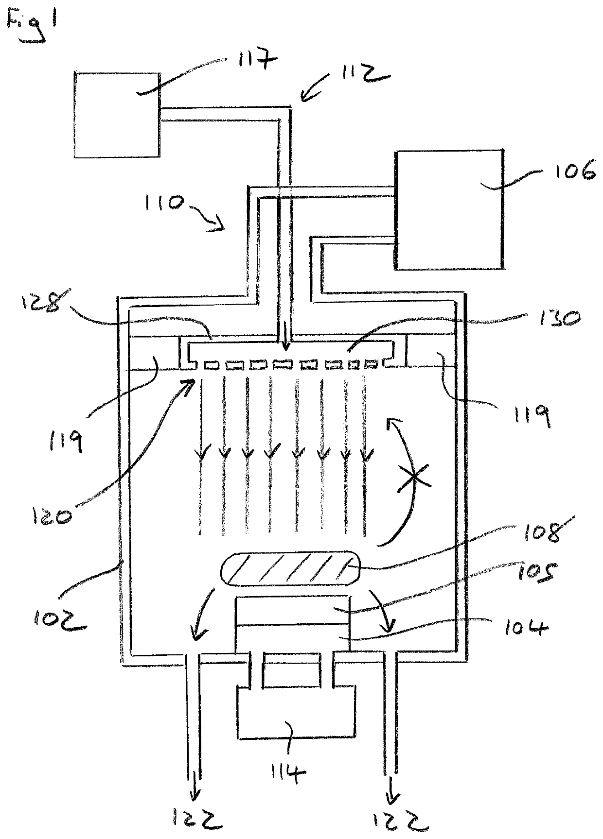
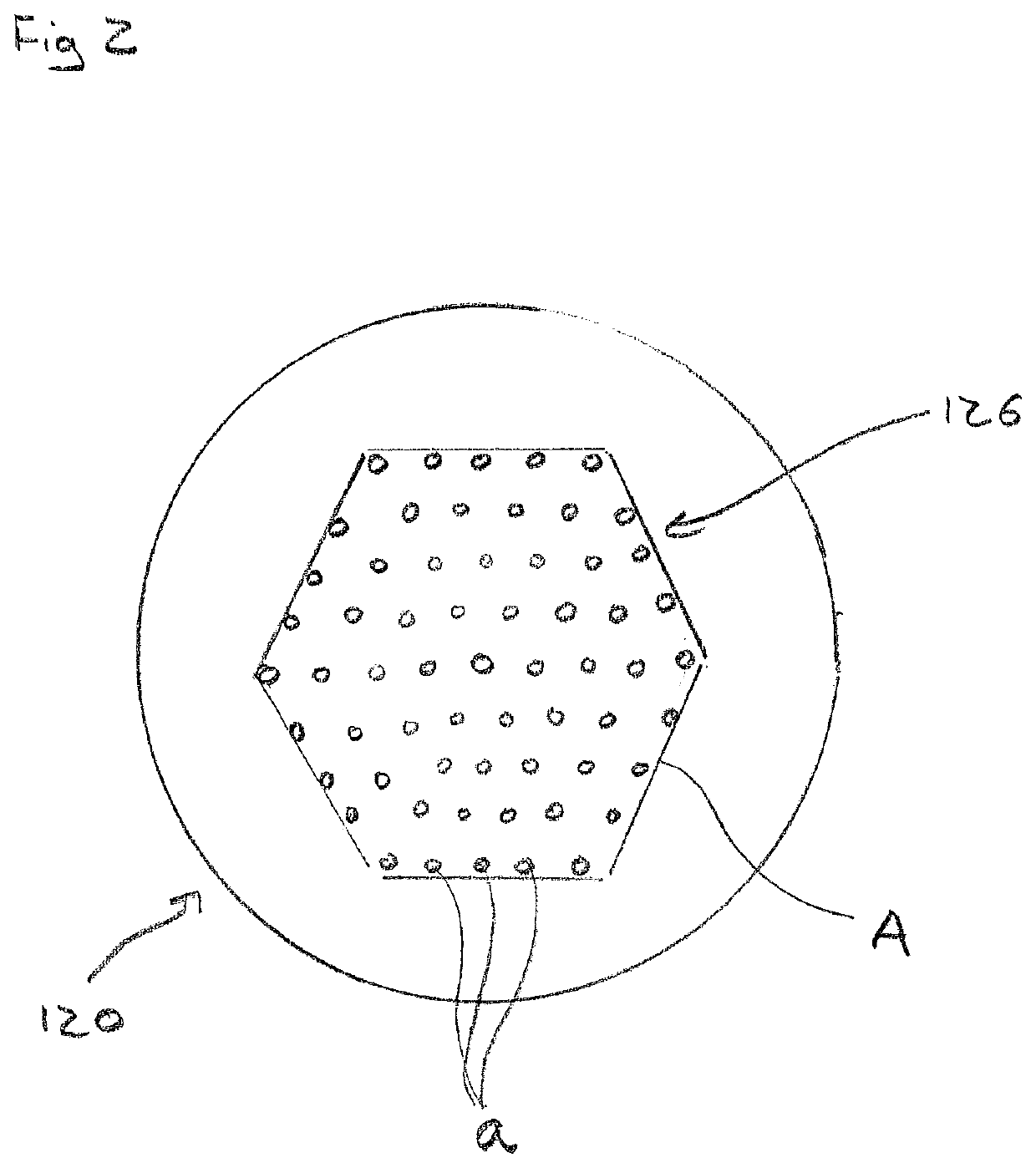
[0058]FIGS. 1 to 3 show various views of a microwave plasma reactor according to an embodiment of the present invention.

[0059]As can be seen by reference to FIG. 1, the microwave plasma reactor comprises the following basic components: a plasma chamber 102; a substrate holder 104 disposed in the plasma chamber for holding a substrate 105; a microwave generator 106 for forming a plasma 108 within the plasma chamber 102; a microwave coupling configuration 110 for feeding microwaves from the microwave generator 106 into the plasma chamber 102 via a coaxial waveguide and through an annular dielectric window 119; a gas flow system 112, 122 for feeding process gases into the plasma chamber 102 and removing them therefrom; and a substrate coolant system 114 for controlling the temperature of a substrate 105.

[0060]It is found that this invention is best utilized in conjunction with simple modal synthesis chambers, for instance the TM011 mode is advantageous as it has been found to be the mo...


PUM

PropertyMeasurementUnit
outlet diameteraaaaaaaaaa

Abstract

A microwave plasma reactor for manufacturing synthetic diamond material via chemical vapour deposition, the microwave plasma reactor includes a plasma chamber, a substrate holder, a microwave coupling configuration for feeding microwaves into the plasma chamber, and a gas flow system for feeding process gases into the plasma chamber and removing them therefrom. The gas flow system includes a gas inlet array having a plurality of gas inlets for directing the process gases towards the substrate holder. The gas inlet array includes at least six gas inlets disposed in a substantially parallel or divergent orientation relative to a central axis of the plasma chamber.

Description

FIELD OF INVENTION[0001]The present invention relates to a microwave plasma reactor for manufacturing synthetic diamond material using chemical vapour deposition techniques.BACKGROUND OF INVENTION[0002]Synthesis of diamond material using chemical vapour deposition (CVD) techniques is now well known. Useful background information relating to the chemical vapour deposition of diamond materials may be found in a special issue of the Journal of Physics: Condensed Matter, Vol. 21, No. 36 (2009) which is dedicated to diamond related technology. For example, the review article by R. S Balmer et al. gives a comprehensive overview of CVD diamond materials, technology and applications (see “Chemical vapour deposition synthetic diamond: materials, technology and applications” J. Phys.: Condensed Matter, Vol. 21, No. 36 (2009) 364221).[0003]A range of possible microwave plasma reactors for diamond film growth via a chemical vapour deposition (CVD) process are known in the art. Such reactors hav...

Claims


Application Information

Patent Timeline
Patent Type & Authority Patents(United States)
IPC IPC(8): C23C16/27C23C16/455C23C16/511H01J37/32C30B29/04C30B25/10
CPCC23C16/45563C23C16/274C23C16/45504C23C16/45565C23C16/511C30B25/105C30B29/04H01J37/32H01J37/3244H01J37/32192H01J37/32238H01J37/32449
Inventor COE, STEVEN EDWARDWILMAN, JONATHAN JAMESTWITCHEN, DANIEL JAMESSCARSBROOK, GEOFFREY ALANBRANDON, JOHN ROBERTWORT, CHRISTOPHER JOHN HOWARD
Owner ELEMENT SIX TECH LTD
Why Eureka
Try Eureka