Semiconductor device

a technology of semiconductor devices and sealing materials, applied in semiconductor devices, semiconductor/solid-state device details, electrical apparatus, etc., can solve the problems of reducing the strength of sealing materials, and cracking of sealing materials

Active Publication Date: 2022-10-04
FUJI ELECTRIC CO LTD
View PDF14 Cites 0 Cited by
  • Summary
  • Abstract
  • Description
  • Claims
  • Application Information

AI Technical Summary

Benefits of technology

[0008]The present inventors studied, in a sealing structure including a primer layer of a polyimide, a polyamide, or the like, to reduce the stress applied to the interface between the primer layer and an electrically conductive connection member by changing the physical property values of a sealing material stacked on the primer layer. It is possible to reduce the interface stress by reducing the content of an inorganic filler which is normally contained in a sealing material to bring the physical property values of the sealing material closer to the physical property values of the primer layer. This makes it possible to secure the adhesion between the sealed member, on which the primer layer is provided, and the primer layer to suppress the decrease in power-cycling capability. On the other hand, there is a risk that reducing the content of the inorganic filler in the sealing material will reduce the strength of the sealing material, leading to cracking of the sealing material. For example, in the case in which the content of the inorganic filler is approximately 70 to 75% by mass relative to the mass of the entire sealing material, the initial strength is also high, so that the degree of decrease in strength is small even after absorption of moisture. However, if the content of the inorganic filler is less than 70%, the initial strength is low, and also the degree of decrease is large after absorption of moisture.
[0009]As a result of earnest studies, the present inventors found that by employing a sealing structure including at least two layers of resins having different compositions and having specific physical properties, it is possible to achieve a better balance between a reduction in interface stress and a high strength, which has been impossible for a single-layer resin sealing structure, and completed the present invention.
[0030]According to the present invention, it is possible to provide a highly reliable semiconductor device in which peeling on an interface between a primer layer and a sealing material is suppressed.

Problems solved by technology

However, in the sealing structure of the conventional power semiconductor module, there is a problem in that repetitive application of thermal stress causes peeling between the sealing material and the sealed members such as the lead frame, cause cracking in the sealing material itself.
On the other hand, there is a risk that reducing the content of the inorganic filler in the sealing material will reduce the strength of the sealing material, leading to cracking of the sealing material.
However, if the content of the inorganic filler is less than 70%, the initial strength is low, and also the degree of decrease is large after absorption of moisture.

Method used


Image

  • Semiconductor device

Examples


examples

[0088](1) Design of Sealing Layers

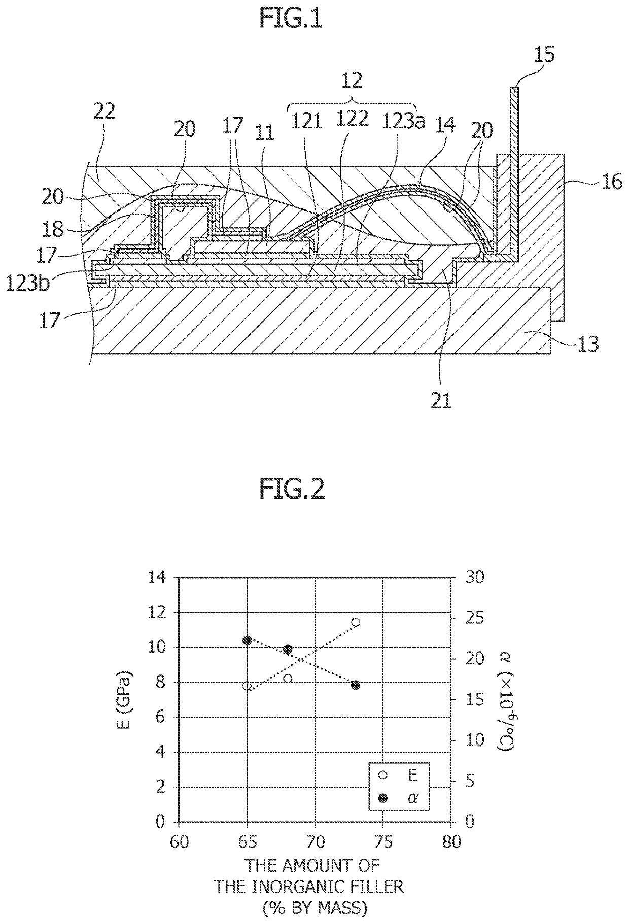
[0089]Thermosetting resin compositions containing an inorganic filler in different contents were prepared, followed by heat curing, and the coefficients of linear thermal expansion and the Young's moduli of the cured products were measured. ME-276 (manufactured by Pelnox Limited) was used as the thermosetting resin base material, and 121% by mass of MV-138 (manufactured by Pelnox Limited) was added to the base material as the acid anhydride-based curing agent. As the inorganic filler, a silica having an average particle size of 10 μm (manufactured by AGC Si-Tech Co., Ltd.) was used. Samples in which the contents of the inorganic filler were 63% by mass, 68% by mass, and 73% by mass relative to the mass of the entire thermosetting resin composition were prepared. These compositions were cured in two stages at 100° C. for 1 hour and at 180° C. for 1 hour to obtain cured products. The coefficient of linear thermal expansion and the Young's modulus were...


PUM

PropertyMeasurementUnit
thicknessaaaaaaaaaa
thicknessaaaaaaaaaa
thicknessaaaaaaaaaa

Abstract

A semiconductor device in which a semiconductor element mounted on a laminate substrate and an electrically conductive connection member are sealed with a sealing material, includes: a primer layer in an interface between the sealing material and sealed members including the laminate substrate, the semiconductor element, and the electrically conductive connection member, in which the sealing material includes a first sealing layer which is provided in contact with the primer layer; and a second sealing layer which covers the first sealing layer, the semiconductor device satisfies αp≥α1>α2 in which αp, α1, and α2 represent coefficients of linear thermal expansion of the primer layer, the first sealing layer, and the second sealing layer, respectively, αc≥15×10−6 / ° C. in which αc represents a composite coefficient of linear thermal expansion of the sealing layers, and Ec≥5 GPa or more in which Ec represents a composite Young's modulus of the sealing layers.

Description

CROSS-REFERENCE TO RELATED APPLICATION[0001]This application claims priority from Japanese Patent Application No. 2020-048029 filed on Mar. 18, 2020, which is incorporated herein by reference in its entirety.BACKGROUND OF THE INVENTIONField of the Invention[0002]The present invention relates to a semiconductor device. The present invention particularly relates to a highly reliable semiconductor device with a longer service life.Description of Related Art[0003]Power semiconductor modules are widely used in fields in which efficient power conversion is required. For example, their application has been expanding to the field of power electronics such as industrial equipment, electric vehicles, and home appliances. These power semiconductor modules incorporate switching elements and diodes, and Si (silicon) semiconductors and SiC (silicon carbide) semiconductors are used for the elements.[0004]A power semiconductor module is manufactured by sealing a chip which is formed of a semiconduc...

Claims


Application Information

Patent Timeline
Patent Type & Authority Patents(United States)
IPC IPC(8): H01L23/29H01L23/31H01L23/42
CPCH01L23/295H01L23/3135H01L23/42H01L2924/181H01L23/3735H01L23/36H01L23/24H01L23/15H01L23/049H01L23/3192H01L23/3171H01L23/3185H01L23/562H01L2224/8592H01L2224/73265H01L2224/40225H01L2224/48091H01L2224/32225H01L2224/40095H01L2224/45124H01L24/45H01L24/40H01L24/48H01L2224/83801H01L2224/84801H01L24/29H01L2224/37655H01L2224/37671H01L2224/37147H01L2224/0603H01L2224/06181H01L24/37H01L2224/8492H01L2224/29101H01L24/84H01L24/85H01L24/83H01L24/73H01L2224/73221H01L2224/73263H01L24/32H01L2224/4569H01L2224/29139H01L2224/83455H01L2224/3749H01L2224/29155H01L2224/29147H01L2224/37471H01L2224/37455H01L2224/2912H01L2224/29111H01L2224/40499H01L2924/00012H01L2924/00014H01L2224/48227H01L2924/014H01L2924/01051H01L2924/0105H01L2924/01029H01L2924/01047H01L2924/01028H01L2924/07025H01L2924/0695
Inventor NAKAMATA, YUKO
Owner FUJI ELECTRIC CO LTD
Why Eureka
Try Eureka