GaN substrate including wide low - defect region for use in semiconductor element

a semiconductor element and substrate technology, applied in semiconductor lasers, crystal growth processes, semiconductor/solid-state device details, etc., can solve the problems of high density of semiconductor laser devices, inability to reliably produce semiconductor laser devices produced by processes, and inability to reliably produce semiconductor laser devices

Inactive Publication Date: 2001-08-23
FUJIFILM HLDG CORP +1
View PDF0 Cites 13 Cited by
  • Summary
  • Abstract
  • Description
  • Claims
  • Application Information

AI Technical Summary

Problems solved by technology

However, the defect density in the semiconductor laser device is still high, and therefore the semiconductor laser device is not reliable in the high output power range.
However, the semiconductor laser device produced by the process is reliable only when the semiconductor laser device operates with the output power of 5 mW or less.
However, in this process, the entire base layer on which the above GaN compound semiconductor layer is grown is formed on a substrate, and the lattice-mismatch between the base layer and the substrate is great.
Therefore, the GaN compound semiconductor layer is affected by the substrate, the crystal orientations of the GaN compound semiconductor layer grown in lateral directions vary, and it is difficult to planarize the surface of the GaN compound semiconductor layer.
Further, even when the above process is repeated, differences arise in the orientations of the crystal faces, and it is therefore impossible to reduce the defect density to a practical level.
However, in this process, the crystal axis is likely to incline due to the mismatch between the sapphire substrate and portions of the GaN layer which are laterally grown over the sapphire substrate, or stress generated in the vicinity of the boundary between the sapphire substrate and the portions of the GaN layer.
Further, as mentioned in Japanese Unexamined Patent Publication No. 11 (1999)-312825, a cavity is formed between the sapphire substrate and the laterally grown portions of the GaN layer, and the formation of the cavity is uncontrollable.
However, since the laterally grown portions of the second GaN layer coalesce in central portions of a plurality of regions which are located above the remaining SiO.sub.2 film of the SiO.sub.2 mask, defects tend to gather in the central portions of the plurality of regions above the remaining Sio.sub.2 film.

Method used


Image

  • GaN substrate including wide low - defect region for use in semiconductor element
  • GaN substrate including wide low - defect region for use in semiconductor element
  • GaN substrate including wide low - defect region for use in semiconductor element

Examples


first embodiment

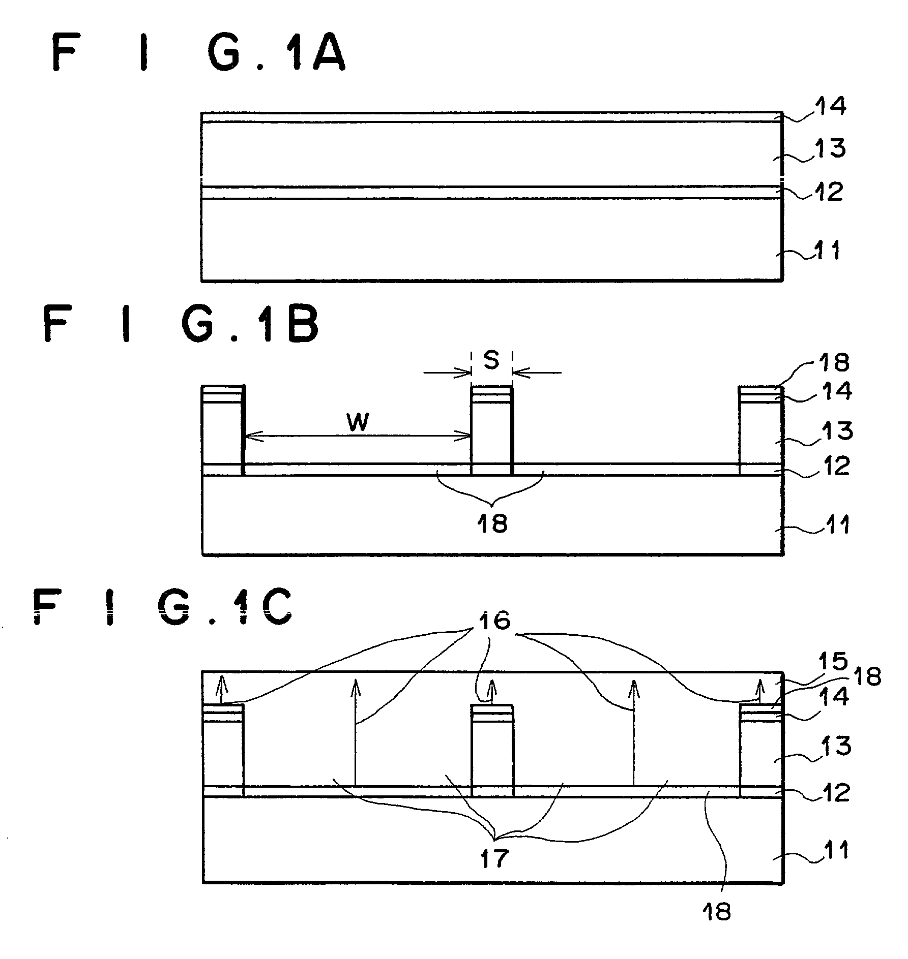
[0048] First Embodiment

[0049] FIGS. 1A to 1C are cross-sectional views of representative stages of a process for producing a semiconductor substrate in the first embodiment of the present invention.

[0050] As illustrated in FIG. 1A, a GaN buffer layer 12 having a thickness of about 20 nm is formed on a (0001) face of a sapphire substrate 11 at a temperature of 500.degree. C. by the normal pressure MOCVD (metal organic chemical vapor deposition) technique using trimethyl gallium (TMG) and ammonia as raw materials. Then, a GaN layer 13 having thickness of about 5 micrometers is formed on the GaN buffer layer 12 at a temperature of 1,050.degree. C. Next, a SiO.sub.2 layer 14 is formed on the GaN layer 13, and a resist film (not shown) is formed on the SiO.sub.2 layer 14. Then, stripe areas of the SiO.sub.2 layer 14 oriented in the direction are removed by the conventional photolithography, so as to form a line-and-space pattern comprised of SiO.sub.2 stripes being spaced with intervals...

second embodiment

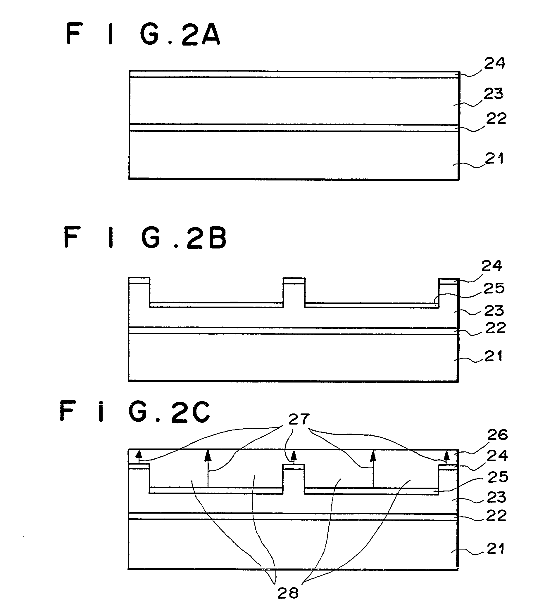
[0055] Second Embodiment

[0056] FIGS. 2A to 2C are cross-sectional views of representative stages of a process for producing a semiconductor substrate in the second embodiment of the present invention.

[0057] As illustrated in FIG. 2A, a GaN buffer layer 22 having a thickness of about 20 nm is formed on a (0001) face of a sapphire substrate 21 at a temperature of 500.degree. C. by the normal pressure MOCVD technique using trimethyl gallium (TMG) and ammonia as raw materials. Then, a GaN layer 23 having thickness of about 5 micrometers is formed on the GaN buffer layer 22 at a temperature of 1,050.degree. C. Next, a SiN.sub.x film 24 is formed on the GaN layer 23, and a resist film (not shown) is formed on the SiN.sub.x film 24. Then, stripe areas of the SiN.sub.x film 24 oriented in the direction are removed by the conventional photolithography, so as to form a line-and-space pattern comprised of SiN.sub.x stripes being spaced with intervals (W) of 25 micrometers and each having a wi...

third embodiment

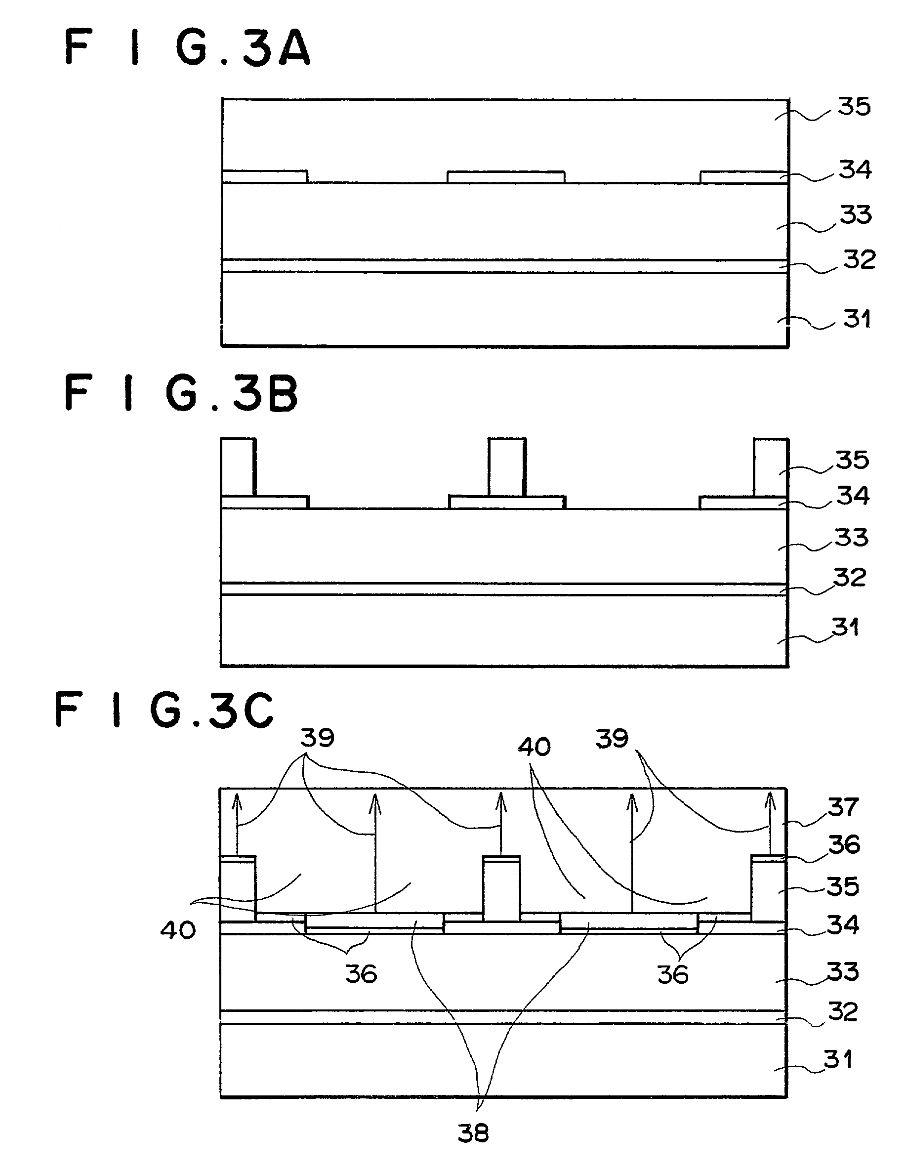
[0060] Third Embodiment

[0061] FIGS. 3A to 3C are cross-sectional views of representative stages of a process for producing a semiconductor substrate in the third embodiment of the present invention.

[0062] As illustrated in FIG. 3A, a low-temperature GaN buffer layer 32 having a thickness of about 20 nm is formed on a sapphire substrate 31 at a temperature of 550.degree. C. by the normal pressure MOCVD technique. Then, a GaN layer 33 is formed on the low-temperature GaN buffer layer 32 at a temperature of 1,050.degree. C. Next, a SiN.sub.x film 34 (having a thickness of about 0.5 micrometers) is formed on the GaN layer 33 by the plasma CVD technique, and a resist film (not shown) is formed on the SiN.sub.x film 34. Then, stripe areas of the SiN.sub.x film 34 oriented in the direction are removed by the conventional photolithography, so as to leave SiN.sub.x stripes 34 being spaced with intervals (W) of 20 micrometers and each having a width of 15 micrometers. Thereafter, a GaN layer...


PUM

PropertyMeasurementUnit
widthaaaaaaaaaa
widthaaaaaaaaaa
output poweraaaaaaaaaa

Abstract

A GaN substrate formed with a substrate, a first GaN layer, a first preventing film, a second GaN layer, and a second preventing film. The first GaN layer is formed on the substrate, and includes a plurality of stripe portions which form at least one first groove between adjacent ones of the plurality of stripe portions. The second GaN layer is formed over the substrate and the first GaN layer. The first preventing film is arranged on upper surfaces of the plurality of stripe portions, and prevents crystal growth of a GaN layer in a vertical up direction from the upper surfaces of the plurality of stripe portions. The second preventing film is arranged on at least one bottom surface of the at least one first groove, and prevents crystal growth of a GaN layer in a vertical up direction from the at least one bottom surface.

Description

[0001] 1. Field of the Invention[0002] The present invention relates to a GaN substrate which is used in a semiconductor element, and in which the defect density is low. The present invention also relates to a process for producing a GaN substrate which is used in a semiconductor element, and in which the defect density is low. The present invention further relates to a semiconductor element including a semiconductor laser device which uses a GaN substrate in which the defect density is low.[0003] 2. Description of the Related Art[0004] S. Nakamura et al. ("Violet InGaN / GaN / AlGaN-Based Laser Diodes Operable at 50.degree. C. with a Fundamental Transverse Mode," Japanese Journal of Applied Physics, vol. 38 (1999) L226-L229) disclose a short-wavelength semiconductor laser device which emits laser light in the 410 nm band.[0005] This semiconductor laser device is formed as follows. First, a GaN substrate is formed by growing a first GaN layer on a sapphire substrate, selectively growing...

Claims


Application Information

Patent Timeline
Patent Type & Authority Applications(United States)
IPC IPC(8): H01L33/06H01L33/12H01L33/14H01L33/32H01L33/44H01S5/02H01S5/323H01S5/343
CPCB82Y20/00H01L33/0075H01S5/0213H01S5/0422H01S5/2231H01S5/3216H01S5/34333H01S2301/173H01S2304/04H01S2304/12
Inventor HAYAKAWA, TOSHIRO
Owner FUJIFILM HLDG CORP
Why Eureka
Try Eureka