Method for producing transparent conductive film, transparent conductive film, transparent conductive substrate and device comprising the same
- Summary
- Abstract
- Description
- Claims
- Application Information
AI Technical Summary
Benefits of technology
Problems solved by technology
Method used
Image
Examples
example 1
[0167][Production of Solution, Liquid A]
[0168]Acetylacetone indium (a full name: tris (acetylacetonato)indium) [In(C5H7O2)3] (molecular weight=412.15) 40 g, p-tert-butyl phenol 42 g, a dibasic acid ester (manufactured by DuPont Japan Limited) 14 g, and hydroxypropyl cellulose (HPC) 4 g were mixed, and the mixture was heated to 130° C., which was stirred for 90 minutes to dissolve it. Next, the obtained solution 25 g, cyclohexanone 25 g, propylene glycol monomethyl ether (PGM) 10 g, and methyl ethyl ketone (MEK) 40 g were mixed and thoroughly stirred until the mixture was uniform, whereby a solution (liquid A) containing the acetylacetone indium and the hydroxypropyl cellulose was produced.
[0169][Production of Solution, Liquid B]
[0170]Acetylacetone tin (a full name: di-n-butoxide bis(2,4-pentanedionate)tin [Sn(C4H9)2(C5H7O2)2] (a molecular weight=431.14) 40 g, p-tert-butyl phenol 42 g, a dibasic acid ester (manufactured by DuPont Japan Limited) 14 g, and hydroxypropyl cellulose (HPC)...
example 2
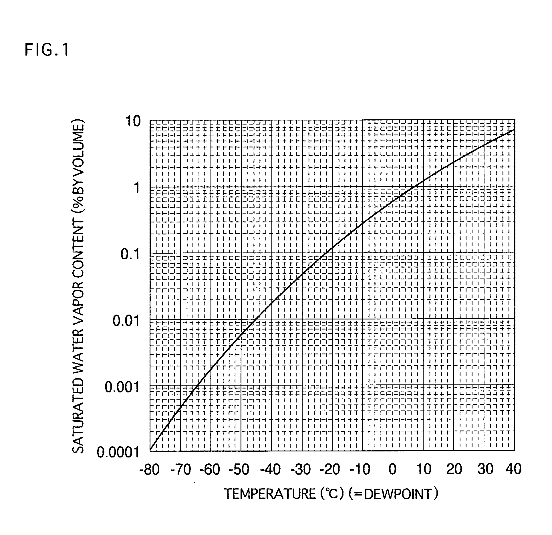
[0183]The same procedure of Example 1 was repeated except that, in the baking using the hot plate in Example 1, the temperature was elevated to 350° C. for 35 minutes (a rate of temperature elevation: 10° C. / minute) under an air atmosphere having a dewpoint of −30° C. (one liter / minute supply), the baking was performed at 350° C. for 15 minutes, only the atmosphere was changed to an atmosphere of 2% hydrogen-98% nitrogen (one liter / minute supply), and the baking was continued at 350° C. for further 15 minutes, whereby a transparent conductive film of Example 2 containing indium oxide (In2O3) as the main component and tin oxide (SnO2) for a dopant was produced.
[0184]The various properties of the transparent conductive film produced were measure in the same manner as in Example 1. The results are shown in Table 1.
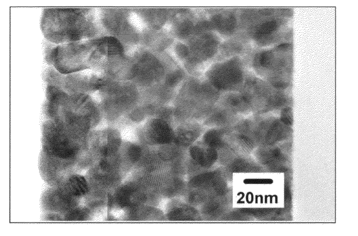
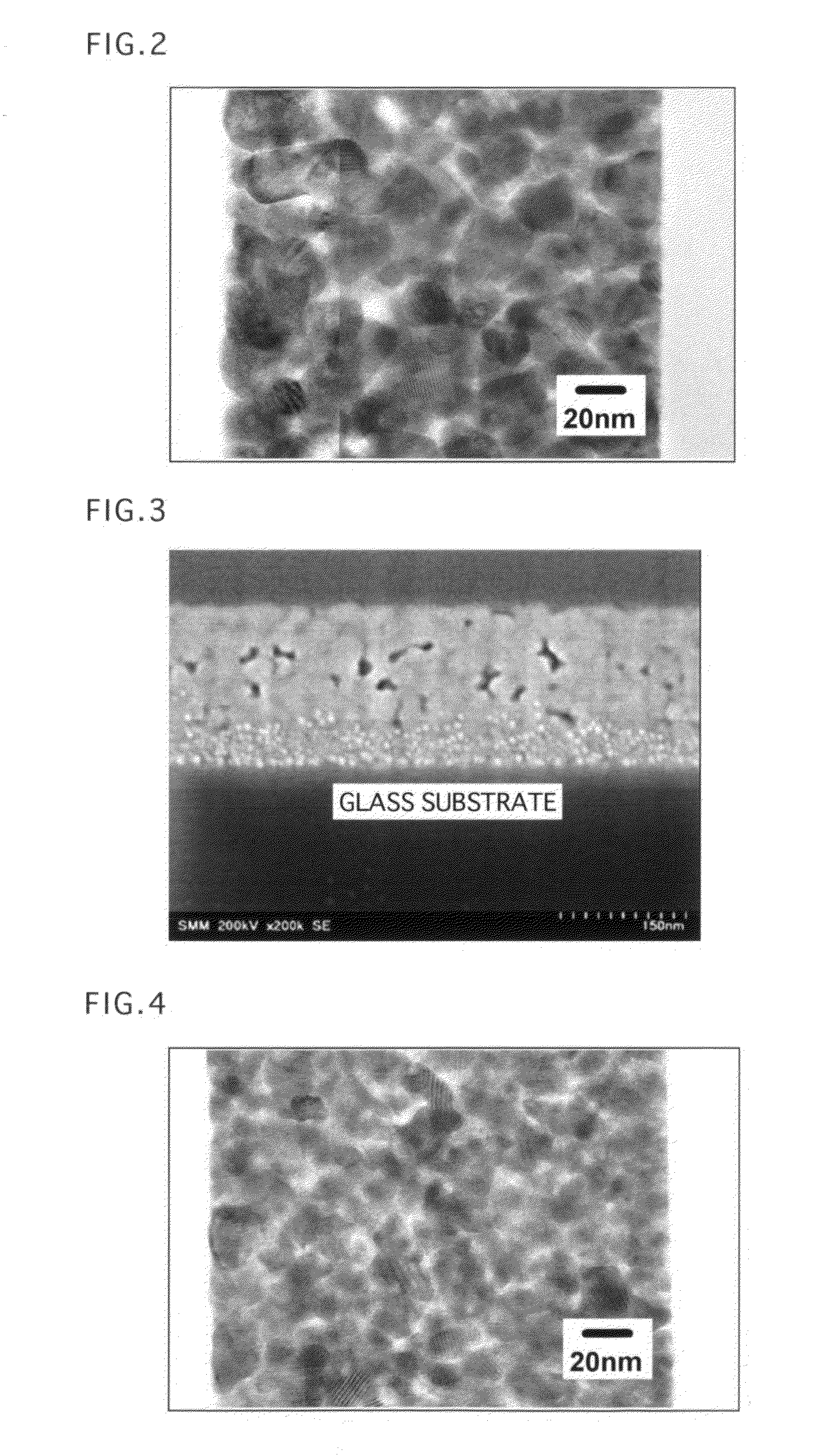
[0185]Further a transmission electron micrograph (a TEM image) and a scanning electron micrograph (a SEM image), obtained by observing the cross-section of the transparent co...
example 3
[0186]A film was produced in the same manner as in Example 1, except that, in the baking using the hot plate in Example 1, an air (air filled in a cylinder) having a dewpoint of −80° C. or lower was used instead of the air having a dewpoint of −30° C., whereby a transparent conductive film of Example 3 containing indium oxide (In2O3) as the main component and tin oxide (SnO2) for a dopant was produced.
[0187]The various properties of the transparent conductive film produced were measured in the same manner as in Example 1, and the results are shown in Table 1.
[0188]Further, when the cross-section of the transparent conductive film of Example 3 was observed with a transmission electron microscope, a conductive oxide microparticle layer that was densely filled with conductive oxide microparticle was observed.
PUM
| Property | Measurement | Unit |
|---|---|---|
| Temperature | aaaaa | aaaaa |
| Temperature | aaaaa | aaaaa |
| Electrical resistance | aaaaa | aaaaa |
Abstract
Description
Claims
Application Information


