

Method of anisotropic etching of substrates
a substrate and anisotropic technology, applied in the direction of basic electric elements, semiconductor/solid-state device manufacturing, electric devices, etc., can solve the problems of inability to achieve anisotropic etching, depletion of ions and radicals, and random direction of ion movement, etc., to achieve stable and repeatable effect, less heat generation, and less ion movemen
- Summary
- Abstract
- Description
- Claims
- Application Information
AI Technical Summary
Benefits of technology
Problems solved by technology
Method used
Image

Examples
Embodiment Construction
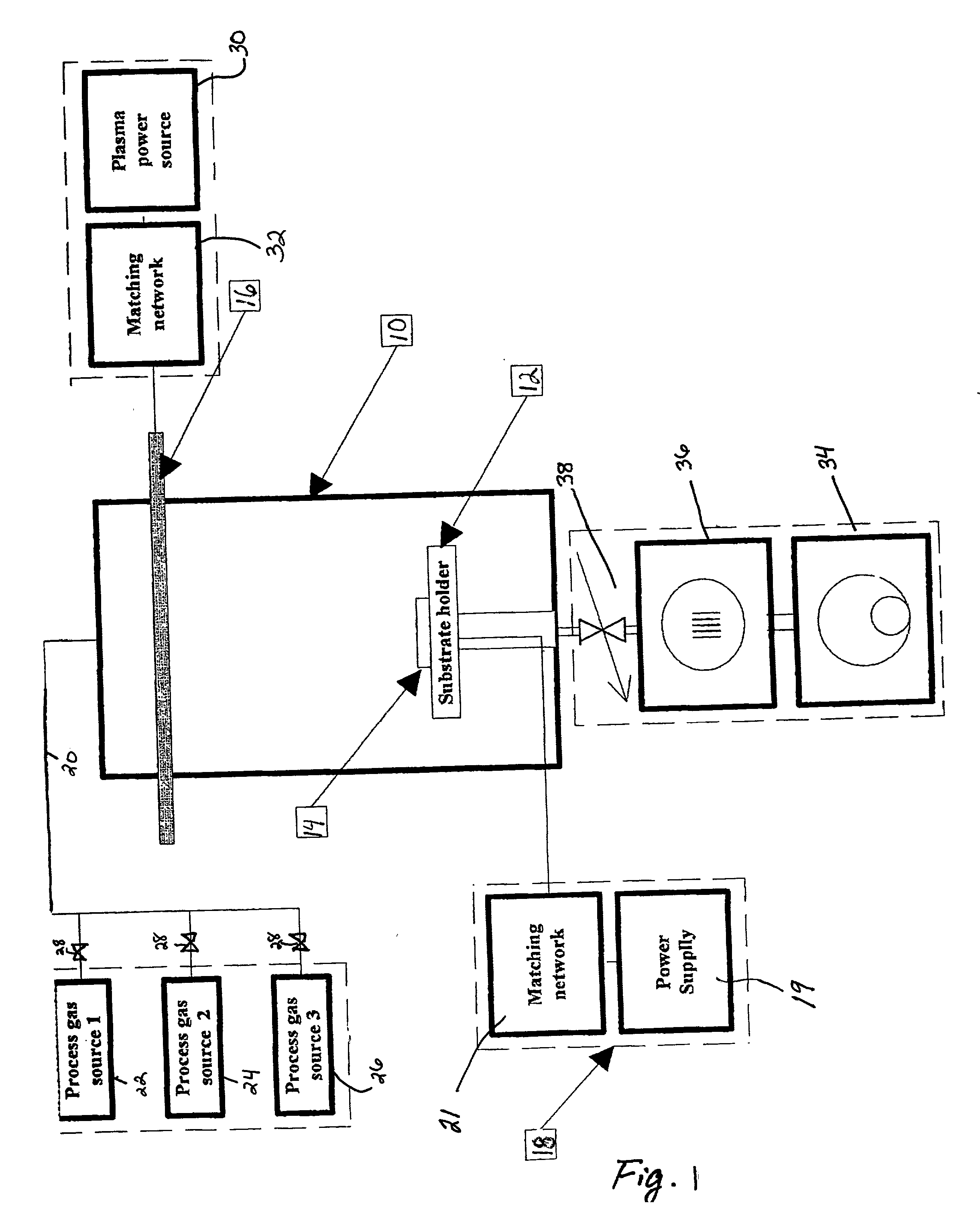
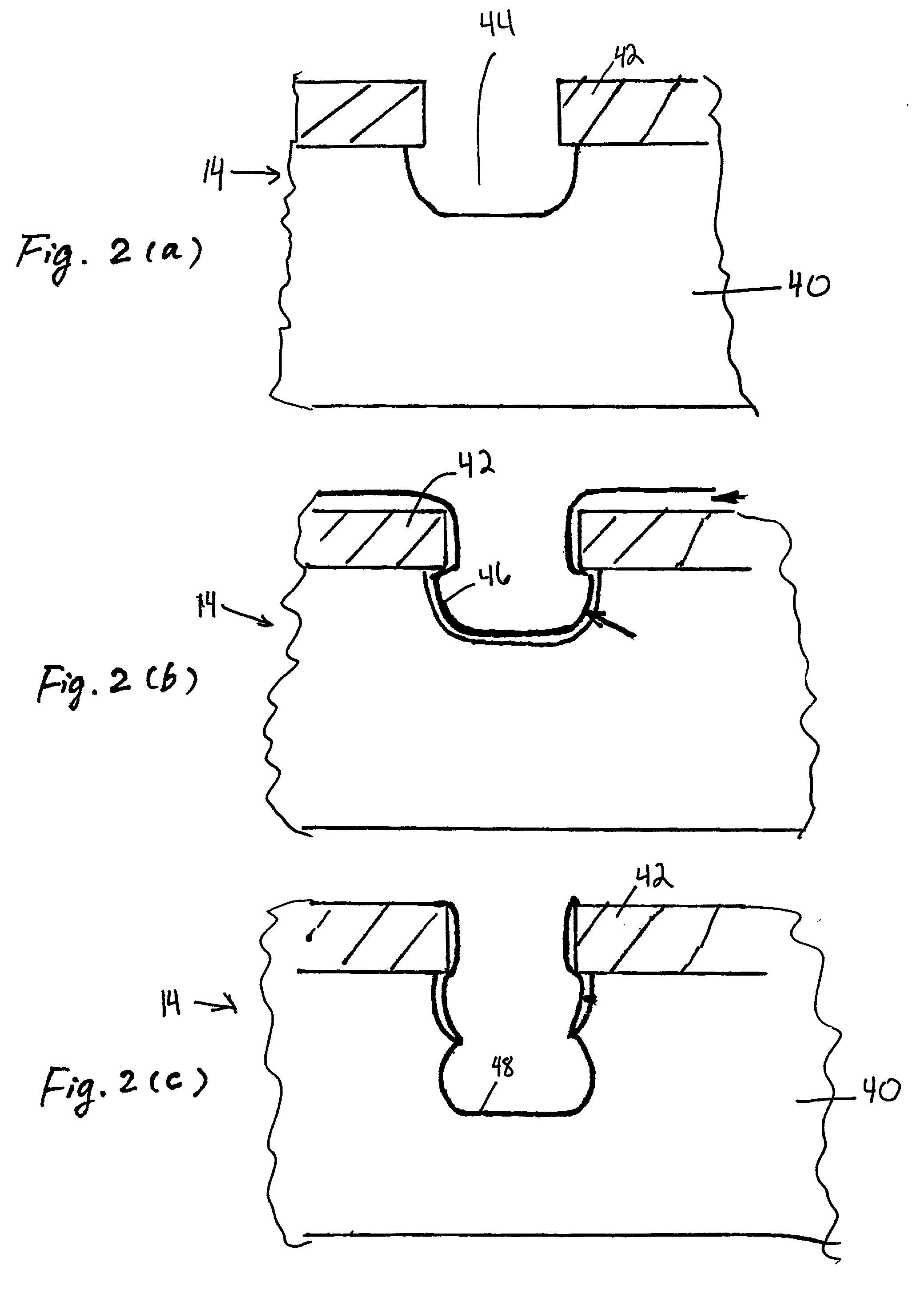
with reference to FIGS. 1 and 2(a) to 2(c). Referring to FIG. 1, the device includes an etching chamber 10. Provided within the chamber 10 is a substrate holder 12 for holding substrate 14 as well as an inductive coupler 16 provided near the top of the chamber 10. The substrate holder 12 is an electrode which is electrically connected to generator 18, including a power supply 19 and a matching network 21, for polarizing the substrate 14. Located at the top of the chamber is an inlet line 20 for introducing process gases into the chamber. The process gases are stored in gas tanks 22, 24 and 26. The flow rate of the process gases into the chamber 10 is controlled by a control valves 28. The plasma stimulation is provided by inductive coupler 16 powered by an RF power source 30 and an associated matching network 32. Pressure within the chamber 10 is controlled by mechanical pump 34, turbo-molecular pump 36 and throttle valve 38, in the conventional manner. It is of course understood th...
PUM
| Property | Measurement | Unit |
|---|---|---|
| gas pressure | aaaaa | aaaaa |
| power | aaaaa | aaaaa |
| power | aaaaa | aaaaa |
Abstract
Description
Claims
Application Information