Method of manufacturing a semiconductor device

a manufacturing method and semiconductor technology, applied in semiconductor devices, instruments, optics, etc., can solve the problems of contaminated substrate surface, difficult to continuously conduct all steps of forming and treating respective films constituting a tft, and damage to the reliability of

Inactive Publication Date: 2002-01-31
SEMICON ENERGY LAB CO LTD
View PDF0 Cites 87 Cited by
  • Summary
  • Abstract
  • Description
  • Claims
  • Application Information

AI Technical Summary

Problems solved by technology

Particularly, that the contaminant impurity exists on an interface of films constituting the TFT is a great factor to damage the reliability of the TFT.
It is difficult to continuously condu

Method used


Image

  • Method of manufacturing a semiconductor device
  • Method of manufacturing a semiconductor device
  • Method of manufacturing a semiconductor device

Examples


embodiment mode 1

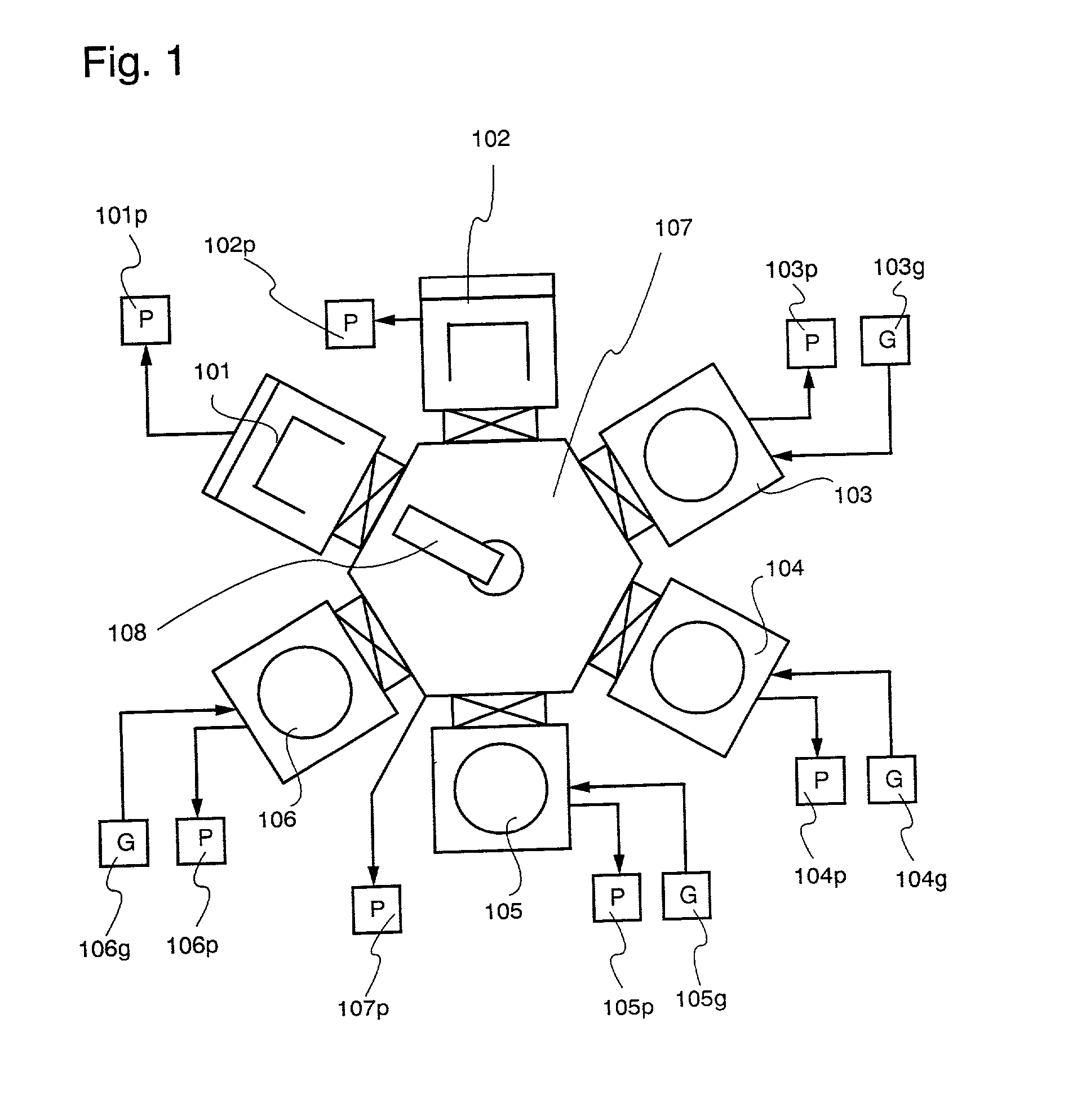
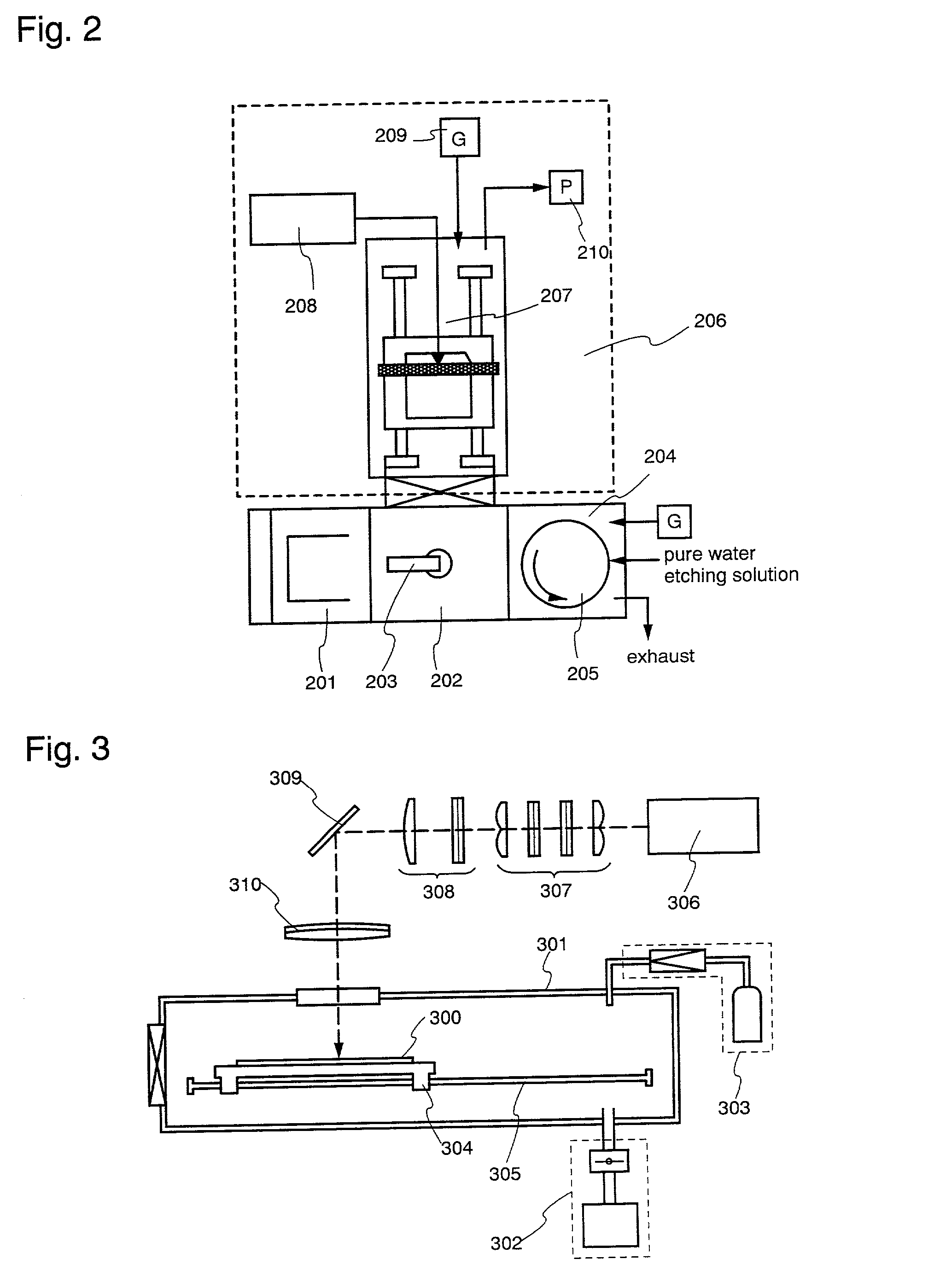
[0046] FIG. 1 shows a film formation apparatus including a plurality of film formation chambers. This film formation apparatus includes loader / unloader chambers 101 and 102, a transfer chamber 107, a transfer robot 108, and film formation chambers 103 to 106. Exhaust systems 101p, 102p and 107p for evacuating the respective chambers are provided for the loader / unloader chambers and the transfer chamber, and lines 103g to 106g for introducing gases used for film formation and exhaust systems 103p to 106p are provided for the film formation chambers.

[0047] The formation of respective films is carried out in the respective film formation chambers. The formation of a base film is carried out in the first film formation chamber 103, and next, the formation of an amorphous semiconductor film is carried out in the second film formation chamber 104, and next, a catalytic element for promoting crystallization of the amorphous semiconductor film is added in the third film formation chamber 10...

embodiment mode 2

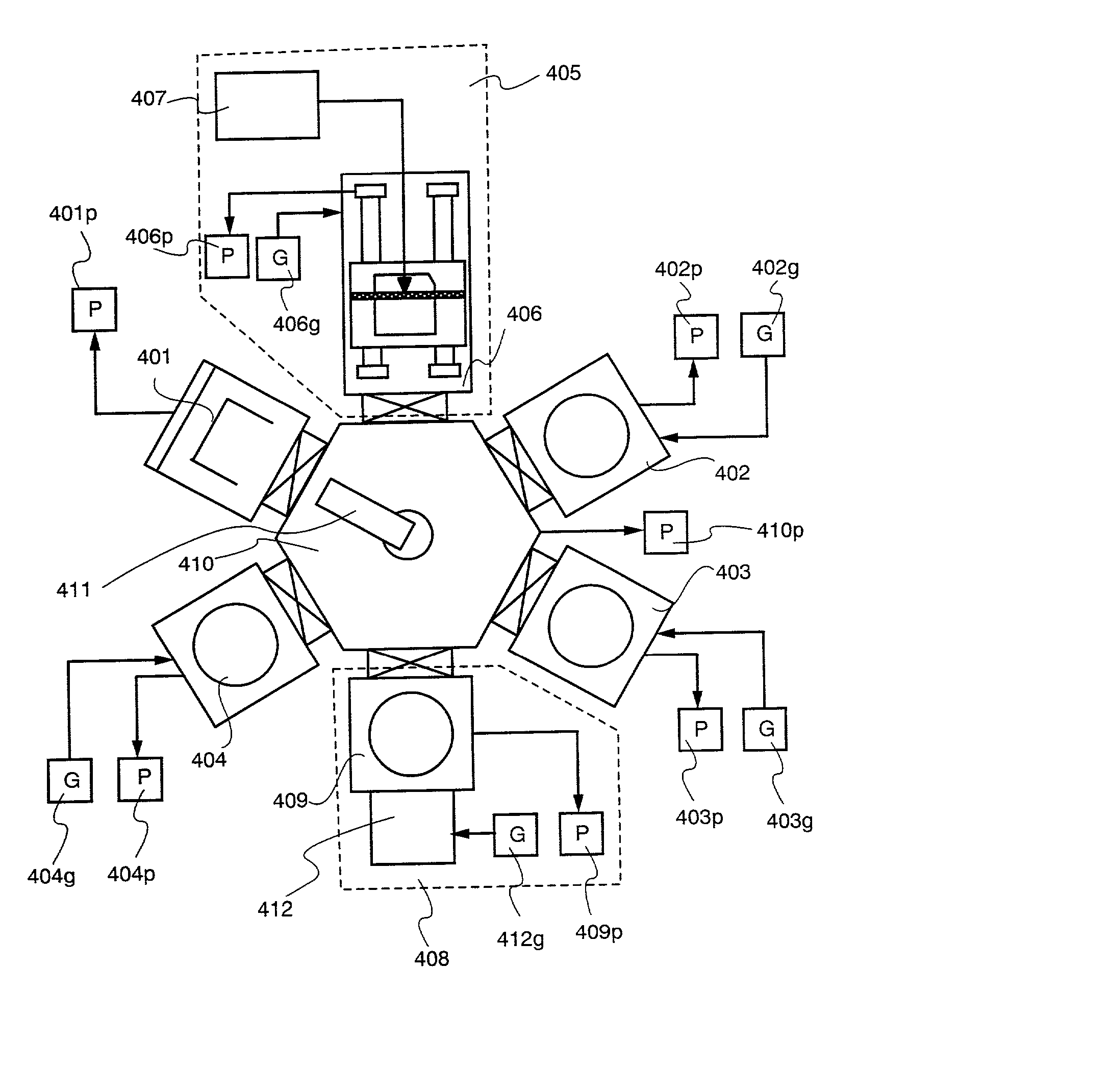
[0053] FIG. 4 shows an apparatus for manufacturing a semiconductor device in which film formation chambers 402 to 404, a laser apparatus 405, and a doping apparatus 408 are connected with one another through a transfer chamber 410. Exhaust systems 401p and 410p for evacuating the respective chambers are provided for a loader / unloader chamber 401 and the transfer chamber 410. Lines 402g to 404g for introducing gases used for film formation and exhaust systems 402p to 404p are provided for the film formation chambers. A substrate is set in the loader / unloader chamber 401. The set substrate is transferred to the respective treatment chambers by a transfer robot 411.

[0054] First, the formation of a base film is carried out in the first film formation chamber 402. Next, an amorphous semiconductor film is formed in the second film formation chamber 403. Next, a first laser annealing is carried out by the laser apparatus 405. It is known that a doped amorphous semiconductor film is difficu...

embodiments

Embodiment 1

[0060] Embodiments of the present invention will be described with reference to FIGS. 5A to 5C, FIGS. 7A to 10, and FIG. 17. In this embodiment, a description will be made of a manufacturing method of simultaneously forming, on the same substrate, a pixel portion and TFTs (n-channel TFT and p-channel TFT) of a driver circuit formed in the periphery of the pixel portion, is described in detail.

[0061] As a substrate 500, a glass substrate, a quartz substrate, a ceramic substrate, or the like may be used. Also, a silicon substrate, a metallic substrate, or a stainless substrate on which an insulating film is formed may be used. A plastic substrate having heat resistance to a process temperature of this embodiment may also be used.

[0062] Then, as shown in FIG. 5A, a base film 501 is formed from an insulating film such as a silicon oxide film, a silicon nitride film or a silicon oxynitride film on a substrate 500. In this embodiment, a two-layer structure is used as the base ...


PUM

PropertyMeasurementUnit
Crystallization enthalpyaaaaaaaaaa

Abstract

Contamination of an interface of respective films constituting a TFT due to an contaminant impurity in a clean room atmosphere becomes a great factor to lower the reliability of the TFT. Besides, when an impurity is added to a crystalline semiconductor film, its crystal structure is broken. By using an apparatus for manufacturing a semiconductor device including a plurality of treatment chambers, a treatment can be made without being exposed to a clean room atmosphere in an interval between respective treatment steps, and it becomes possible to keep the interface of the respective films constituting the TFT clean. Besides, by carrying out crystallization after an impurity is added to an amorphous semiconductor film, the breakdown of the crystal structure of the crystalline semiconductor film is prevented.

Description

[0001] 1. Field of the Invention[0002] The present invention relates to a method of manufacturing a semiconductor device, such as a thin film transistor (hereinafter referred to as a TFT), using a crystalline semiconductor film formed on a substrate. The semiconductor device fabricated by the present invention includes not only an element such as a TFT or a MOS transistor, but also a liquid crystal display device, an EL (Electro Luminescence) display device, an EC (Electro Chromic) display device, an image sensor, or the like, each including a semiconductor circuit (microprocessor, signal processing circuit, high frequency circuit, etc.) constituted by insulated gate transistors.[0003] 2. Description of the Related Art[0004] At present, as a semiconductor element using a semiconductor film, a thin film transistor (hereinafter referred to as a TFT) is used for each integrated circuit, and is especially used as a switching element of an image display device. Further, a TFT using as an...

Claims


Application Information

Patent Timeline
IPC IPC(8): G02F1/136G02F1/1368H01L21/20H01L21/304H01L21/336H01L27/12H01L29/49H01L29/786
CPCH01L21/2022H01L27/12H01L29/4908H01L29/66757Y10T29/41H01L29/78621H01L29/78684H01L2029/7863H01L29/66765H01L21/02532H01L21/02672
Inventor YAMAZAKI, SHUNPEIASAMI, TAKETOMIICHIJO, MITSUHIROMITSUKI, TORUKANAKUBO, YOKO
Owner SEMICON ENERGY LAB CO LTD
Why Eureka
Try Eureka