Semiconductor device provided with semiconductor circuit made of semiconductor element and method of fabricating the same

a semiconductor element and semiconductor device technology, applied in the direction of transistors, optics, instruments, etc., can solve the problems of difficult control of the concentration of impurities, large fluctuations in tft characteristics, and difficult control of tft characteristics, so as to improve the characteristics of tft, improve the interface, and uniform characteristics

Inactive Publication Date: 2005-06-02
SEMICON ENERGY LAB CO LTD
View PDF74 Cites 17 Cited by
  • Summary
  • Abstract
  • Description
  • Claims
  • Application Information

AI Technical Summary

Benefits of technology

[0013] An object of the present invention is to enhance characteristics of a TFT by improving an interface between an active layer, especially a region making a channel formation region and an insulating film, and to provide a semiconductor device provided with a semiconductor circuit made of a semiconductor element having uniform characteristics and a method of fabricating the same.
[0014] Another object of the present invention is to provide a semiconductor device provided with a semiconductor circuit made of a semiconductor element with an LDD structure which is high in reproducibility, improves stability of transistor characteristics, and is high in productivity, and a method of fabricating the same.
[0015] In order to achieve the above objects, one of the features of the present invention is that at least a gate insulating film and a semiconductor film are formed without exposing them to an atmosphere onto an insulating surface on which a gate wiring line is formed, next, crystallization by irradiation of infrared light or ultraviolet light (laser light) is carried out, and then, doping of an impurity is carried out, so that a source region and a drain region are formed. The doping of the impurity is carried out through an insulating film covering the semiconductor film. That is, the feature of the present invention is that when a TFT of a bottom gate structure (typically, inverted stagger structure) is formed, a same chamber or a multichamber apparatus, for example, a system as shown in FIG. 13 is used so that the semiconductor film to become the active layer is prevented from being exposed to the atmosphere. By such structure, pollution of the interface of the active layer is prevented, and stable and excellent electrical characteristics are realized.
[0032] Moreover, one of the features of the present invention is that an LDD region is formed by using, for example, a photosensitive organic material film, a silicon oxide film, or the like as a mask on a protective film. Furthermore, the present invention is characterized in that an active layer, especially a channel formation region is protected against deterioration due to light by using the mask used for formation of the LDD structure as a light shielding film, and a removing step of the mask is omitted. In addition, at a crossing portion of a gate wiring line and other wiring lines, the mask functions as an insulating film, so that interwiring capacitance can be reduced.

Problems solved by technology

However, although a TFT having an active layer of a crystalline semiconductor film is superior in operation speed and driving capability as compared with a TFT having an active layer of an amorphous semiconductor film, it has a problem that fluctuation in TFT characteristics is large.
If this interface is polluted, the TFT characteristics are badly affected.
When boron is mixed into the active layer like this, it becomes difficult to control the concentration of impurities in the active layer, which causes the fluctuation of threshold values of TFTs.
In the case where another filter is used, the cost becomes so high that this is not suitable.
When a semiconductor element, for example, a TFT is fabricated by using the semiconductor film polluted in this way, characteristics of an interface between the active layer, especially a channel formation region and the gate insulating film are degraded, which causes fluctuation and deterioration of electrical characteristics of TFTs.
Besides, also in a crystallizing step, the impurities (boron, oxygen, moisture, sodium, etc.) hinder crystallization of the semiconductor film.
However, a method of fabricating an LDD structure using a conventional technique is complicated, and many steps are required.

Method used


Image

  • Semiconductor device provided with semiconductor circuit made of semiconductor element 
and method of fabricating the same
  • Semiconductor device provided with semiconductor circuit made of semiconductor element 
and method of fabricating the same
  • Semiconductor device provided with semiconductor circuit made of semiconductor element 
and method of fabricating the same

Examples


embodiment 1

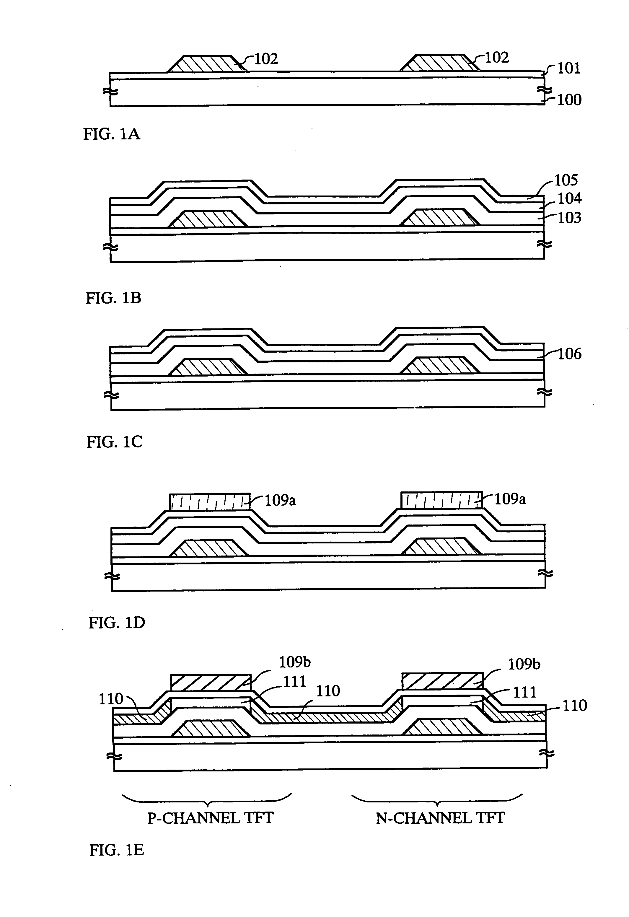
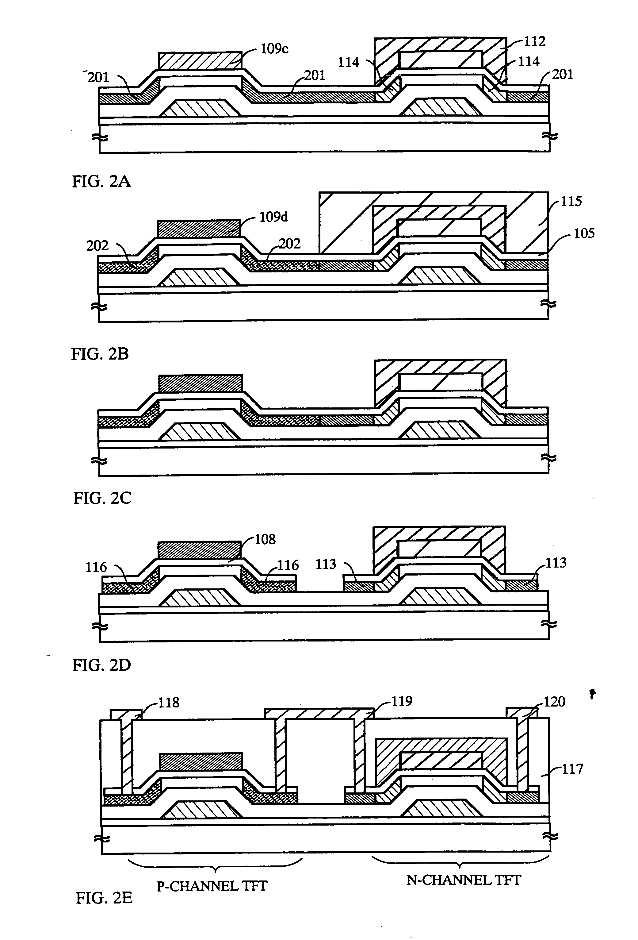
[0059] In this embodiment, an example of a case where an inverted stagger type TFT is fabricated by using the present invention will be described. In this embodiment, a description will be made using a CMOS circuit constituted by an N-channel TFT and a P-channel TFT.

[0060] The brief description will be made using FIGS. 1 to 4 which are simplified sectional views showing a semiconductor device of the present invention and a method of fabricating the same.

[0061] First, a substrate 100 is prepared. As the substrate 100, an insulating substrate such as a glass substrate, a quartz substrate, or a crystalline glass substrate, a ceramic substrate, a stainless substrate, a metal (tantalum, tungsten, molybdenum, etc.) substrate, a semiconductor substrate, a plastic substrate (polyethylene terephthalate substrate), or the like can be used. In this embodiment, a glass substrate (Corning 1737; distortion point 667° C.) was used as the substrate 100.

[0062] Next, an under film 101 is formed on...

embodiment 2

[0106] This embodiment is an example in which a crystalline silicon film is obtained by a method different from the embodiment 1. This embodiment relates to a method in which a catalytic element for promoting crystallization of silicon is used, a laser beam is shaped into a rectangle or square, and a crystalline silicon film is obtained through a uniform laser crystallization process over a region of several cm2 to several hundred cm2 by one shot of irradiation. Since the basic structure is almost the same as the embodiment 1, a description will be made while paying attention to only different points.

[0107] In this embodiment, in the step of FIG. 1C, excimer laser light is processed into a plane shape and irradiation is made. In the case where laser light is processed into the plane shape, it is necessary to process the laser light so that an area of about several tens cm2 (preferably 10 cm2 or more) can be irradiated at the same time. For the purpose of annealing the whole irradia...

embodiment 3

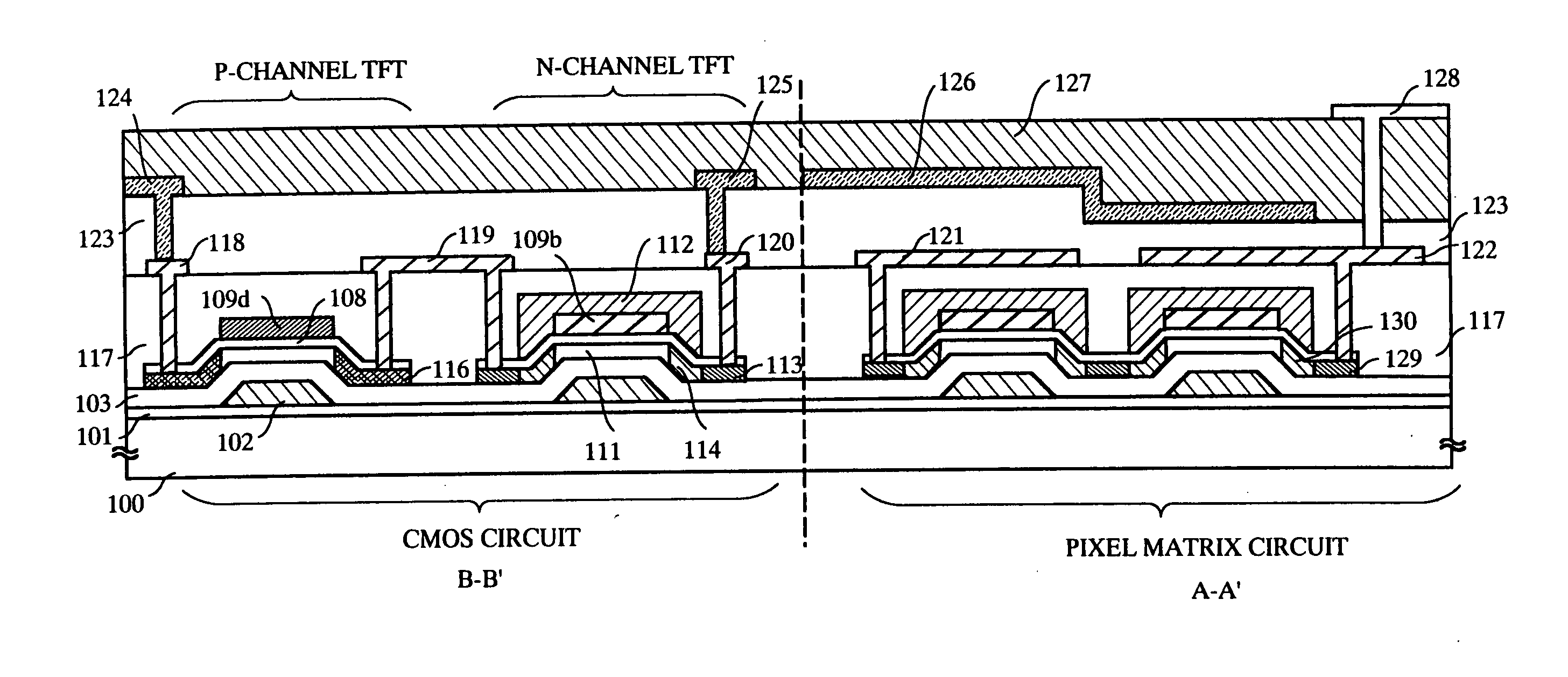
[0111] In this embodiment, an example in which a TFT having a structure different from the embodiment 1 will be described with reference to FIG. 5. A top view of FIG. 5 is almost the same as FIG. 4A or 4B, although the reference numerals are different.

[0112] In this embodiment, a plastic substrate is formed as a substrate 500, a silicon nitride oxide (expressed as SiOxNy) is formed as an under film 501, and a tantalum film is formed as a gate wiring line 502.

[0113] Next, as a first insulating film 503, a film of an organic material to flatten the roughness between a region including a gate electrode and a region including no gate electrode, for example, a BCB (benzocyclobutene) film with a thickness of 100 nm to 1 μm (preferably 500 to 800 nm) is formed. In this step, it is necessary to make the film have a thickness to such a degree that a roughened portion due to the gate wiring line 502 is completely flattened. Since the flattening effect of the BCB film is large, sufficient fl...


PUM

PropertyMeasurementUnit
sizeaaaaaaaaaa
thicknessaaaaaaaaaa
thicknessaaaaaaaaaa

Abstract

This invention improves TFT characteristics by making an interface between an active layer, especially a region forming a channel formation region and an insulating film excellent, and provides a semiconductor device provided with a semiconductor circuit made of a semiconductor element having uniform characteristics and a method of fabricating the same. In order to achieve the object, a gate wiring line is formed on a substrate or an under film, a gate insulating film, an initial semiconductor film, and an insulating film are formed into a laminate without exposing them to the atmosphere, and after the initial semiconductor film is crystallized by irradiation of infrared light or ultraviolet light (laser light) through the insulating film, patterning is carried out to obtain an active layer and a protection film each having a desired shape, and then, a resist mask is used to fabricate the semiconductor device provided with an LDD structure.

Description

BACKGROUND OF THE INVENTION [0001] 1. Field of the Invention [0002] The present invention relates to a structure of a semiconductor device provided with a semiconductor circuit made of a semiconductor element such as an insulated gate type transistor, and a method of fabricating the same. Particularly, the invention relates to a structure of a semiconductor device provided with a semiconductor circuit made of a semiconductor element having an LDD structure formed by using organic resin, and a method of fabricating the same. The semiconductor device of the present invention includes not only a element such as a thin film transistor (TFT) or a MOS transistor, but also a display device including a semiconductor circuit constituted by these insulated gate type transistors or an electro-optical device such as an image sensor. In addition, the semiconductor device of the present invention includes also an electronic equipment having these display device and electro-optical device. [0003] ...

Claims


Application Information

Patent Timeline
Patent Type & Authority Applications(United States)
IPC IPC(8): G02F1/1362H01L21/336H01L21/77H01L21/84H01L27/12H01L29/786
CPCG02F1/13454G02F1/136227H01L27/1214H01L29/78678H01L29/78621H01L29/78627H01L29/66765H01L27/1274H01L27/1296
Inventor YAMAZAKI, SHUNPEINAKAJIMA, SETSUOKAWASAKI, RITSUKO
Owner SEMICON ENERGY LAB CO LTD
Why Eureka
Try Eureka