
Protection circuit of field effect transistor and semiconductor device

a protection circuit and field effect technology, applied in the direction of emergency protection arrangements for limiting excess voltage/current, electronic switching, pulse technique, etc., can solve the problems of affecting the operation of the protection circuit, the surge resistance of the gate electrode or the drain electrode is extremely low, and the above described conventional protection circuits have problems

Inactive Publication Date: 2002-02-14
SONY CORP
View PDF1 Cites 14 Cited by
  • Summary
  • Abstract
  • Description
  • Claims
  • Application Information

AI Technical Summary

Problems solved by technology

Especially, in the compound semiconductor field effect transistor, such as a JFET, a MESFET, or an HFET, used for a power amplifier, a bias adjusting circuit of an antenna switch or the like and having a small gate width, for example, a gate width of 10 .mu.m to 20 .mu.m, the surge resistance of a gate electrode or a drain electrode is extremely low, and there is a case where the withstanding resistance of the gate electrode or the drain electrode is damaged by a surge voltage of 20 V to 30 V.
However, the above described conventional protection circuits have problems as described below, respectively.
As a result, there is a problem that to make the gate terminal and the drain terminal approach each other becomes a restriction to a pattern layout, and is not preferable in the pattern layout.
In the protection circuit of the conventional example 2, there is a problem that desired surge resistance can not be secured.
Meanwhile, in the case of a compound semiconductor FET in which a laminate structure of compound semiconductor layers is epitaxially grown on a compound semiconductor substrate, such a step of separately adjusting a channel concentration in order to form a protection element can not be carried out because of the process.
In such a case, although it is necessary to further reduce a DC withstand voltage of a diode as a protection element, it becomes impossible to narrow a distance between junctions of the diode in the pattern layout.
On the other hand, although the DC withstand voltage can be made low by providing a Schottky electrode or a pn junction electrode in, for example, an n.sup.+ region having a high doping concentration, that is, a high carrier concentration, there is a problem that a leak current is increased at the same time.

Method used


Image

  • Protection circuit of field effect transistor and semiconductor device
  • Protection circuit of field effect transistor and semiconductor device
  • Protection circuit of field effect transistor and semiconductor device

Examples


embodiment 2

of Embodiment 2

[0075] This modified example is a modified example of the embodiment 2, and FIG. 4 is a circuit diagram of a protection circuit of a field effect transistor of this modified example.

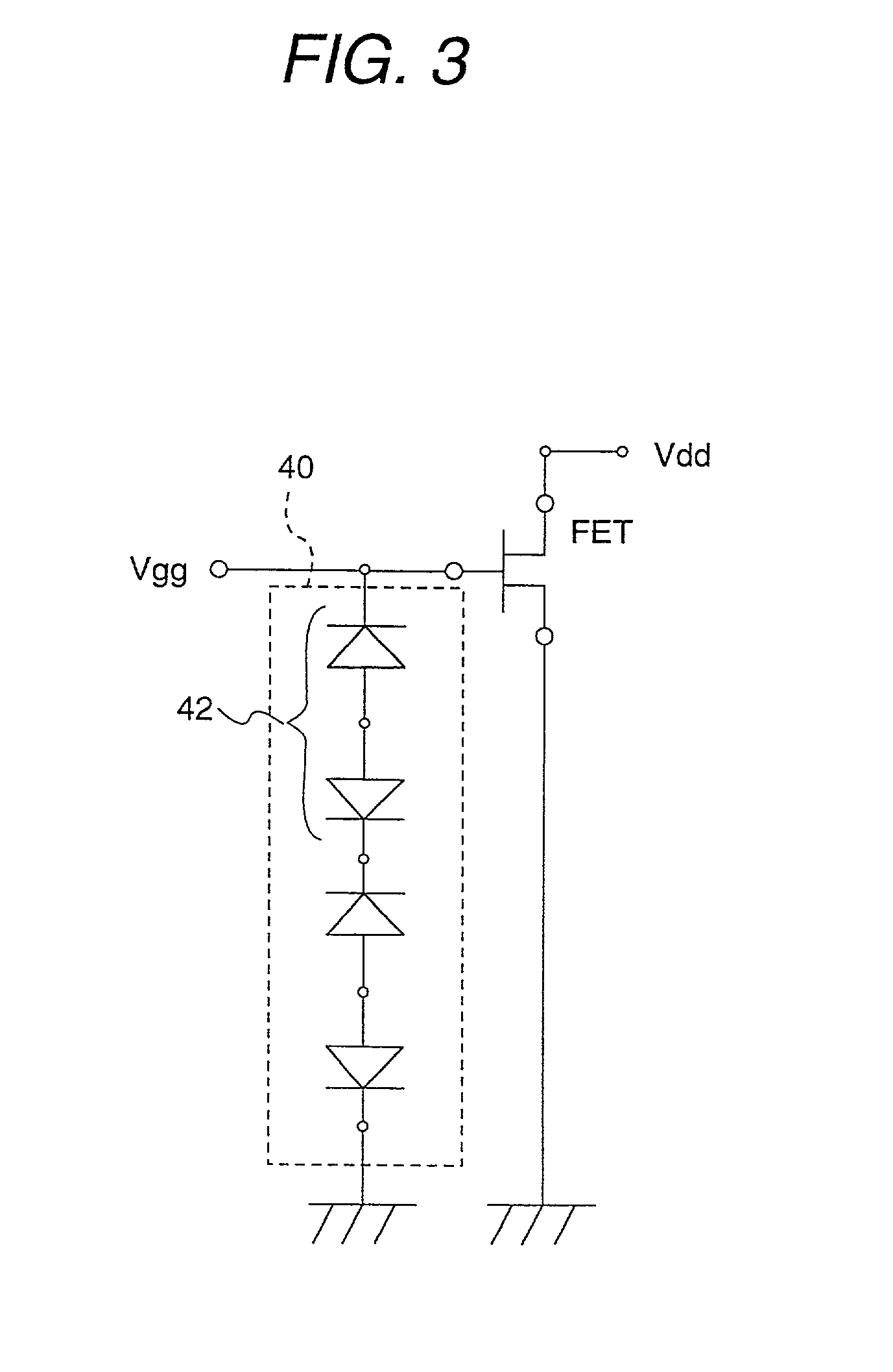
[0076] A protection circuit 50 of a field effect transistor of this modified example is, as shown in FIG. 4, a protection circuit of an FET in which a diode array including two cascade-connected pn junction diodes 52 and a diode array including two cascade-connected np junction diodes 54 are connected in series, and a gate line Vgg connected to a gate electrode of the FET is grounded through the protection circuit 50.

[0077] Also in this modified example, the carrier concentration of an n-type layer of the np junction is preferably made 2.times.10.sup.18 cm.sup.-3 or higher.

modified example 2

[0078] Modified Example 2 of Embodiment 2

[0079] This modified example is another modified example of the embodiment 2, and FIG. 5 is a circuit diagram of a protection circuit of a field effect transistor of this modified example.

[0080] In a protection circuit 60 of a field effect transistor of this modified example, the arrangement of forward direction diodes and reverse direction diodes is opposite to the protection circuit 50 of the modified example 1, and as shown in FIG. 5, it is a protection circuit of an FET in which a diode array including two cascade-connected reverse direction np junction diodes 62 and a diode array including two cascade-connected forward direction pn junction diodes 64 are connected in series. A gate line Vgg connected to a gate electrode of the FET is grounded through the protection circuit 60.

[0081] Also in this modified example, the carrier concentration of an n-type layer of the np junction is preferably made 2.times.10.sup.18 cm.sup.-3 or higher.

embodiment 3

[0082] Embodiment 3

[0083] This embodiment is a protection circuit in which a pn junction diode is made a protection element, instead of the Schottky barrier diode of the embodiment 1.

[0084] Incidentally, as an FET (HFET) including a hetero junction, there is a device as disclosed in, for example, Japanese Patent Unexamined Publication No. Hei. 11-150264 (Japanese Patent Application No. Hei. 9-249217). Here, a structure of the HFET disclosed in the publication will be described with reference to FIG. 6. FIG. 6 is a sectional view showing the structure of the HFET.

[0085] An HFET 70 of this embodiment includes, as shown in FIG. 6, a laminate structure of a buffer layer 74, a second barrier layer 76 made of AlGaAs, a channel layer 78 made of InGaAs, and a first barrier layer 80 made of AlGaAs, sequentially formed on a GaAs substrate 72.

[0086] The first barrier layer 80 is constituted by a carrier supply region 80a containing an n-type impurity, a high resistance region 80b containing no...


PUM


Abstract

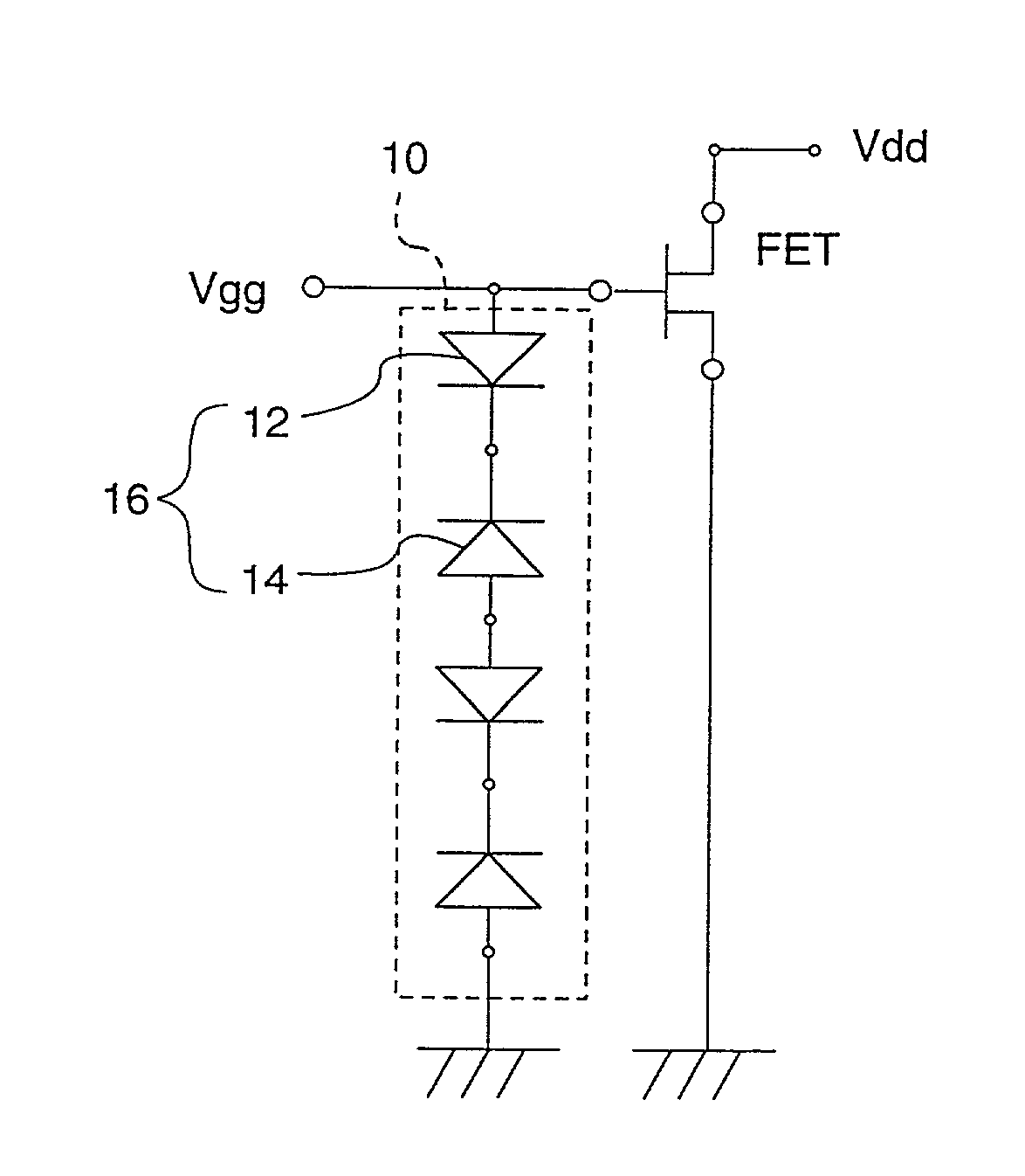
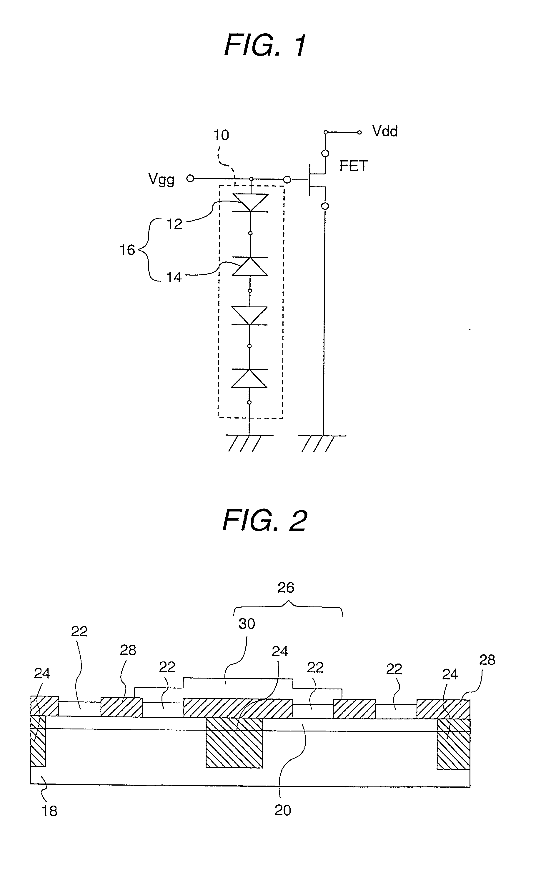
There is provided a protection circuit of a field effect transistor having a structure which can be fabricated without restricting a pattern layout and without increasing a process step. A protection circuit of a field effect transistor is a protection circuit of a Schottky gate HFET, and is a circuit in which a forward direction diode and a reverse direction diode are cascade-connected to form a diode unit and two such diode units are connected in series, and a gate line connected to a gate electrode of the HFET is grounded through the protection circuit. The diodes are diodes formed integrally with the Schottky gate HFET which is protected against surge breakdown, and are constituted as Schottky barrier diodes made of an n+-GaAs cap layer formed on a GaAs substrate and Schottky electrodes formed on the n+-GaAs cap layer.

Description

RELATED APPLICATION DATA[0001] The present invention claims priority to Japanese Application No. P2000-150350 filed May 2,2 2000, which application is incorporated herein by reference to the extent permitted by law.[0002] 1. Field of the Invention[0003] The present invention relates to a protection circuit of a field effect transistor and a semiconductor device provided with the protection circuit, and particularly to a protection circuit of an FET for protecting a gate electrode or a drain electrode of the field effect transistor, especially a JFET, a MESFET, an HFET, or the like against surge breakdown, and for raising the surge resistance of the FET, in which a diode formed integrally with the FET is made a protection element in order to reduce the number of required process steps, and a semiconductor device provided with such a protection circuit.[0004] 2. Description of the Related Art[0005] Since a field effect transistor of a compound semiconductor including a laminate struct...

Claims


Application Information

Patent Timeline
Patent Type & Authority Applications(United States)
IPC IPC(8): H01L21/338H01L27/04H01L21/822H01L27/02H01L29/812H03K17/0812
CPCH01L27/0255H03K17/08122
Inventor NAKAMURA, MITSUHIROWADA, SHINICHI
Owner SONY CORP
Learn More