

Pb-free solder-connected structure and electronic device
- Summary
- Abstract
- Description
- Claims
- Application Information
AI Technical Summary
Benefits of technology
Problems solved by technology
Method used
Image

Examples
example 2
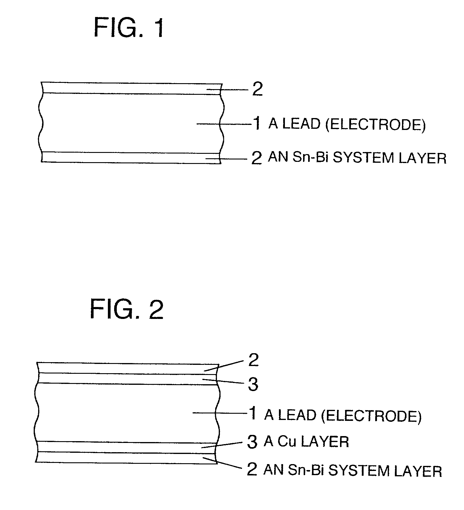
[0053] The cross-sectional structure of a TSOP lead is shown in FIG. 2 which is a part of the lead structure. A Cu layer 3 is formed on a lead 1 which is of an Fe--Ni alloy (42 alloy) and an Sn--Bi alloy layer 2 is formed on this Cu layer. The Sn--Bi alloy layer 3 and Sn--Bi layer 2 were formed by plating. The thickness of the Cu layer 3 was about 8 .mu.m and that of the Sn--Bi plating layer was about 10 .mu.m. The Bi content of Sn--Bi alloy plating layer was 5 wt %. Because of high rigidity of the TSOP lead, when it is used at a high temperature or under a condition that heat generation occurs in the device itself, stress generated at the interface is greater as compared with the QFP-LSI. In such cases, it is necessary to form an interface with sufficient bonding strength high enough to withstand this interface stress and the Cu layer under the Sn--Bi layer is effective for this purpose.
[0054] The TSOP was soldered to a printed-circuit board in a vapor reflow furnace with utilizati...
example 3
[0055] The electrode structures according to this invention can also be applied in an electrode on a board. For example, solder coating is effective in improving the solderability of boards. Conventionally, there have been used lead-containing solders such as a eutectic Sn--Pb alloy solder. Thus, the Sn--Bi alloy layer according to the invention can be used to make the solder for coating lead-free. Furthermore, because the electrode of a board is made of copper, sufficient bonding strength can be obtained when an Sn--Ag--Bi alloy solder is used. An example in which this structure is applied is shown; an Sn--8 Bi alloy layer of about 5 .mu.m was formed by roller coating on a Cu pad (Cu electrode) on a glass epoxy substrate, which is a circuit board,
[0056] Wettability to boards and bonding strength were improved, because the solder layer was formed.
Industrial Applicability
[0057] An electrode structure can be realized, which is suitable for an Sn--Ag--Bi alloy solder excellent as a lea...
PUM
| Property | Measurement | Unit |
|---|---|---|
| Structure | aaaaa | aaaaa |
| Electrical resistance | aaaaa | aaaaa |
| Strength | aaaaa | aaaaa |
Abstract
Description
Claims
Application Information