Semiconductor flip-chip package and method for the fabrication thereof

Inactive Publication Date: 2002-03-14
INVENSAS CORP
View PDF0 Cites 84 Cited by
  • Summary
  • Abstract
  • Description
  • Claims
  • Application Information

AI Technical Summary

Benefits of technology

0060] The semiconductor chip package structures of the present invention provide, among other advantages, simple chip placement followed by reflow without labor intensive underfill steps; a solder bumped chip or substrate with an encapsulant pre-attached, with the encapsulant performing a mechanic

Problems solved by technology

One obstacle to flip-chip technology when applied to polymer printed circuit substrates (i.e., circuit boards) is the unacceptably poor reliability of the solder joints due to the mismatch of the coefficients of thermal expansion of the (i) chip, which typically has a coefficient of thermal expansion of about 3 ppm/.degree. C., (ii) the polymer substrate, e.g. epoxy-glass, which has a coefficient of thermal expansion of about 16 to 26 ppm/.degree. C., and (iii) the solder joint which has a coefficient of thermal expansion of about 25 ppm/.degree. C. As shown in FIGS. 2 and 3, as the flip chip 100 and printed circuit substrate 101 undergo thermal excursions, the substrate expands and contracts at a greater rate than does the ch
oints. As the chip and substrate are thermally cycled through normal use, this flexing and bending weakens the solder joints which causes them to quickl
The underfilling process, however, makes the assembly of encapsulated flip-chip printed wire boards a time consuming, labor intensive and expensive process with a number of uncertainties.
After reflow, due to the close proximity of the chip to the substrate, removing any remaining flux residues from under the chip is such a difficult operation that it is generally not done.
Yet these residues are known to reduce the reliability and integrity of the subsequent underfill encapsulant.
Typically, the filler to resin volume ratio is in the range of 50 to 65%, but this high filler concentration tends to make the resin mixture very viscous, which slows the rate at which it can flow into the gap between chip and substrate during underfilling.
Consequently, the slow und

Method used


Image

  • Semiconductor flip-chip package and method for the fabrication thereof
  • Semiconductor flip-chip package and method for the fabrication thereof
  • Semiconductor flip-chip package and method for the fabrication thereof

Examples


example 1

(Preparation of Encapsulant that is suitable for use as the Second Portion Encapsulant 39 in FIG. 16)

[0094] The entitled encapsulant, comprising a polymer flux, was prepared from a mixture that contained:

[0095] 1. 25 grams bisphenol A glycerolate di(2-octen-1-ylsuccinic) acid monoester;

[0096] 2. 12.5 grams of bisphenol A epoxy; and

[0097] 3. 4 grams of glycidyl 4-nonylphenyl ether.

[0098] This composition was mixed and cured for 4 hours at 165.degree. C. It produced a solid having a thermal coefficient of expansion of about 180 ppm / .degree. C.

example 2

(Preparation of Two-Portion Liquid Underfill Encapsulants Applied Before Assembly)

[0099] A set of ten flip chip assemblies was fabricated. Specifically, a bumped semiconductor chip, part FBT-250 available from Flip Chip Technologies, Phoenix, Ariz., was coated with a first portion liquid encapsulant 111 as shown FIG. 10. The first portion of the encapsulant consisted of a liquid layer, approximately 50 to 75 microns thick, that covered the underside of the chip and the solder bumps completely. It was formed from a mixture that contained:

[0100] 1. Bisphenol A epoxy 15 weight %;

[0101] 2. Glycidyl 4-nonylphenyl ether 6 weight %;

[0102] 3. Pentaeryethritol triacrylate 18 weight %

[0103] 4. Tert-butyl peroxide 0.06 weight %;

[0104] 5. Glass spheres 40 weight % (Aldrich catalog No. 44,034-5); and

[0105] 6. Bisphenol A glycerolate di(2-octen-1-ylsuccinic) acid monoester 20.94 weight %.

[0106] The composition was mixed and cured for 4 hours at 165.degree. C. It produced a solid having a thermal ...

example 3

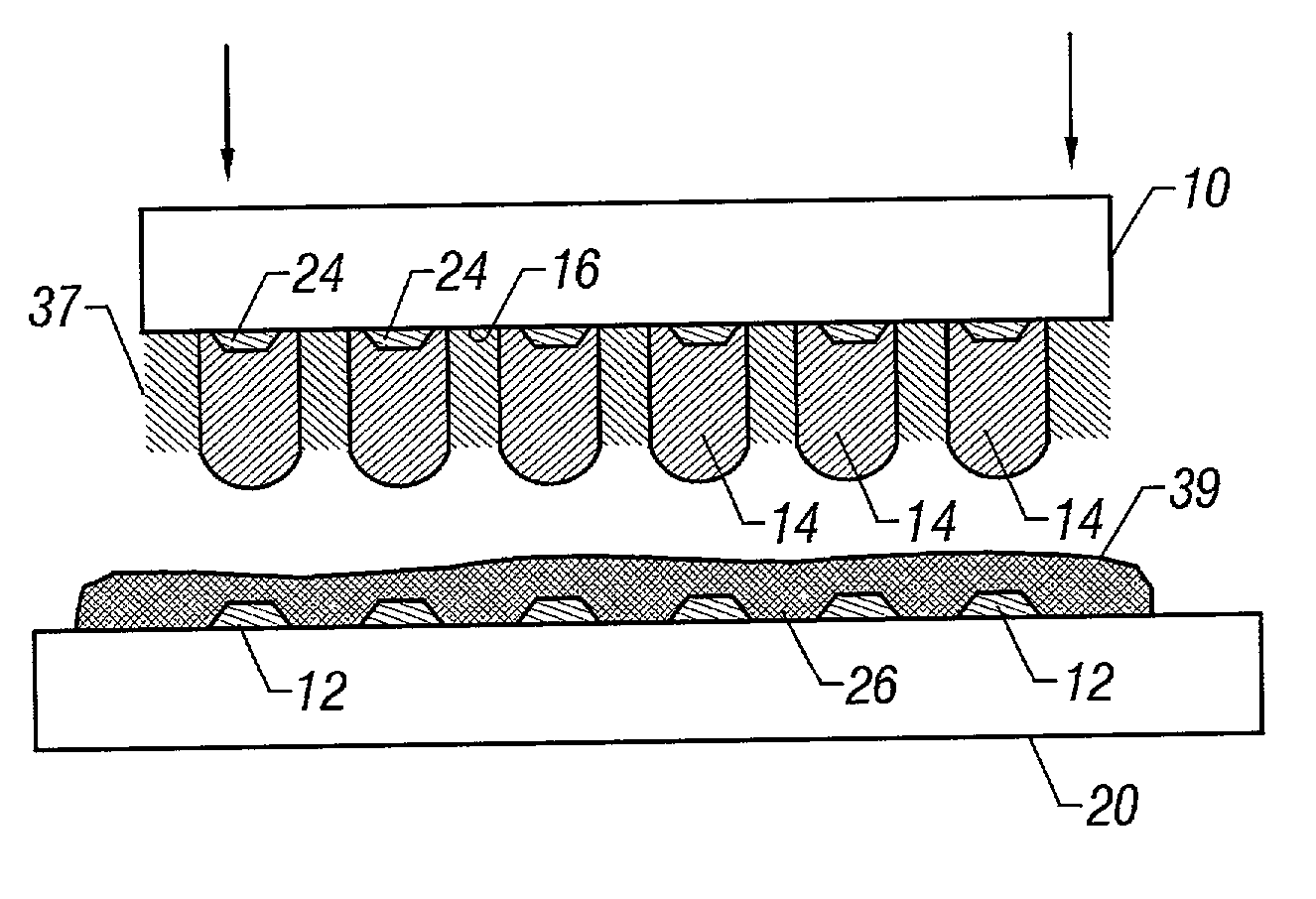
(Preparation of Encapsulant that is Suitable for use as the first Portion Encapsulant 37 in FIG. 16)

[0110] 2-allyl phenyl glycidyl ether was synthesized by heating 2-allyl phenol (AP) and 10 times excess molar ratio epichlorohydrin (EPH) to 115.degree. C. under nitrogen in the presence of aqueous sodium hydroxide (NaOH). During the reaction, water which must be removed is formed by the reaction between 2-AP and EPH. Since water and EPH form an azeotrope, water was removed from the reaction by azeotropic distillation, which to drives the reaction forward. Collected EPH was returned as needed to the mixture to prevent undesirable side reactions. After 4 hours, the resultant salts were separated from the product. The product was then purified by extraction of the oil phase with toluene, followed by removing the excess EPH and aqueous phase with toluene, which was also used as an azeotropic agent. The product obtained was a thin, yellowish, transparent liquid. Yield was about 90%. Disti...


PUM


Abstract

A flip-chip device and process for fabricating the device employs a multilayer encapsulant that includes a first portion encapsulant having a coefficient of thermal expansion of at most 30 ppm/.degree. C. and an elastic modulus of 2-20 GPa and a second portion comprising a polymer flux having a coefficient of thermal expansion that may exceed 30 ppm/.degree. C.

Description

[0001] This application is a divisional of applicationi Ser. No. 09 / 517,839 filed on Mar. 2, 2000, which is a continuation-in-part of application Ser. Nos. 09 / 120,172 and 09 / 137,971, filed Jul. 21, 1998 and Aug. 21, 1998, respectively, and which are incorporated herein in their entiretiesFIELD OF THE INVENTION[0003] This invention relates generally to semiconductor chips electrically and mechanically connected to a substrate, particularly to flip-chip configurations.BACKGROUND OF THE INVENTION[0004] Flip-chip technology is well known in the art. FIG. 1 illustrates a semi-conductor chip having solder bumps formed on the active side of the semi-conductor chip 100 that is inverted and bonded to a substrate 101 through the solder joints 102 by reflowing solder to wet metallized pads 106. Structural solder joints 102 are formed from solder bumps situated between the semi-conductor chip and the substrate to form the mechanical and electrical connections between the chip and substrate. A n...

Claims


Application Information

Patent Timeline
IPC IPC(8): H01L21/56H01L23/498
CPCH01L21/563H01L23/49827H01L2224/16225H01L2224/274H01L2224/73203H01L2224/73204H01L2224/83193H01L2924/01002H01L2924/01005H01L2924/01011H01L2924/01027H01L2924/01029H01L2924/01039H01L2924/01049H01L2924/0105H01L2924/01078H01L2924/01079H01L2924/01082H01L2924/01327H01L2924/14H01L2924/3511H01L2924/01006H01L2924/01023H01L2924/01033H01L2924/014H01L24/29H01L24/32H01L2224/32225H01L2924/00H01L2924/12042H01L2224/73104H01L2224/1148H01L2224/05573H01L2224/05568H01L2224/056H01L24/05H01L2924/00014
Inventor CAPOTE, MIGUEL ALBERTZHU, XIAOQIBURRESS, ROBERT VINSONLEE, YONG-JOON
Owner INVENSAS CORP
Why Eureka
Try Eureka