
Method of manufacturing group iii-v compound semiconductor

Inactive Publication Date: 2002-04-18
SUMITOMO CHEM CO LTD
View PDF0 Cites 9 Cited by
  • Summary
  • Abstract
  • Description
  • Claims
  • Application Information

AI Technical Summary

Problems solved by technology

However, in such a compound semiconductor manufactured by MOVPE, it is known that it is difficult to control the p-type conductivity while it is relatively easy to control the n-type conductivity.
Hence, while it is essential to perform such post-processing to manufacture an element which has a high current injection characteristic, such post-processing unavoidably deteriorates the yield.
Still, this method aims at growing Mg-doped GaN on InGaN which was already grown, and therefore, the Mg-doped GaN does not exhibit the p-type conductivity if an InGaN layer is not used, according to the gazette.
If the carrier gas contains more than 0.5% of hydrogen in capacity, the p-type conductivity is not good enough, which is not desirable.
Further, even though carrier gas which does not contain hydrogen is used while growing a semiconductor, the semiconductor may not exhibit the p-type conductivity in some cases if the atmosphere contains hydrogen while the semiconductor is cooled down.
If the carrier gas according to the present invention is used from the beginning of the growth of crystal, the quality of the crystal may deteriorate, with a surface of the crystal not completed as a mirror surface or other problem.
When mixed with each other, Group V materials and Group III materials may produce an adduct with a low vapor pressure, resulting in a deterioration in the crystal perfection such as a deterioration in the surface morphology.

Method used

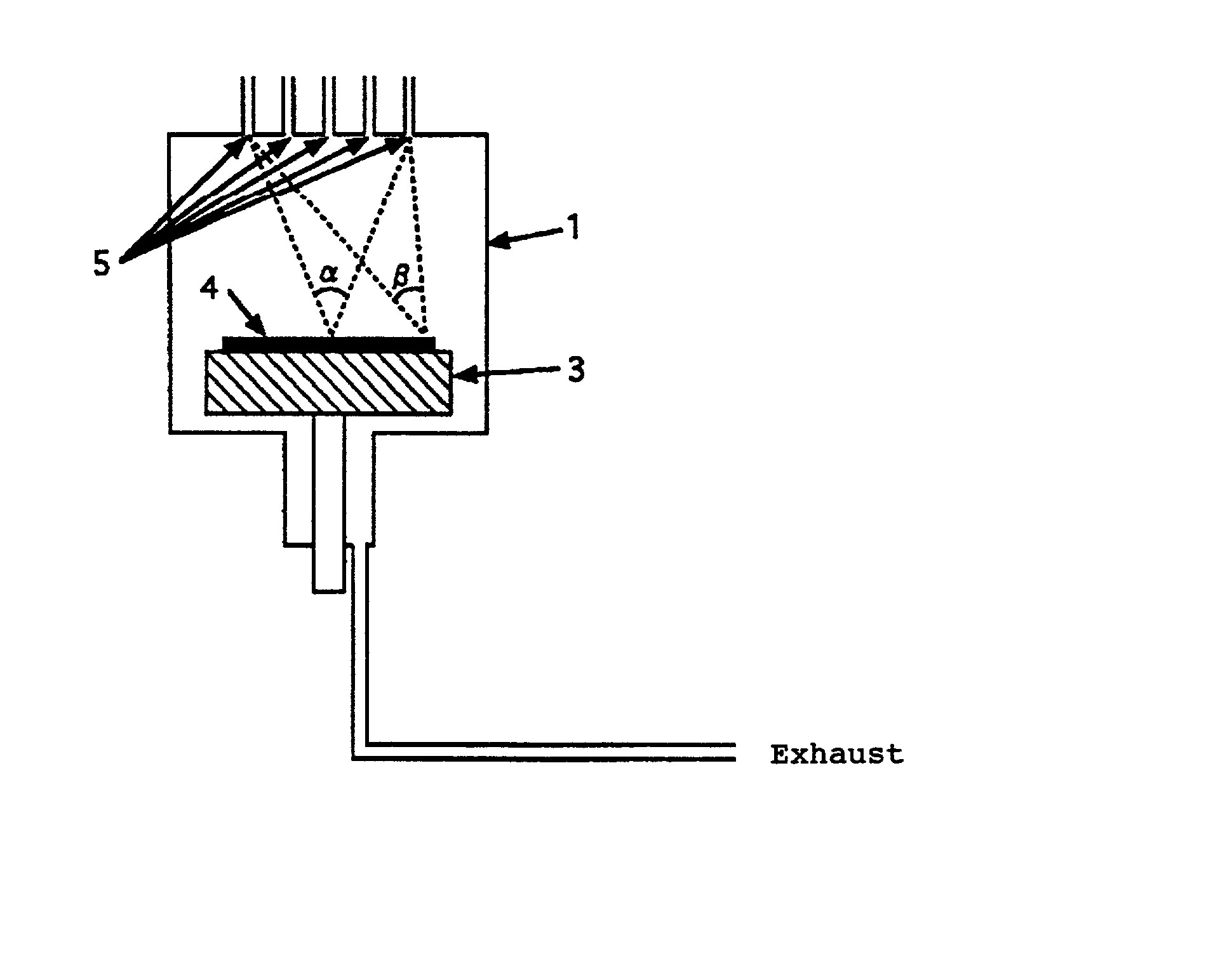
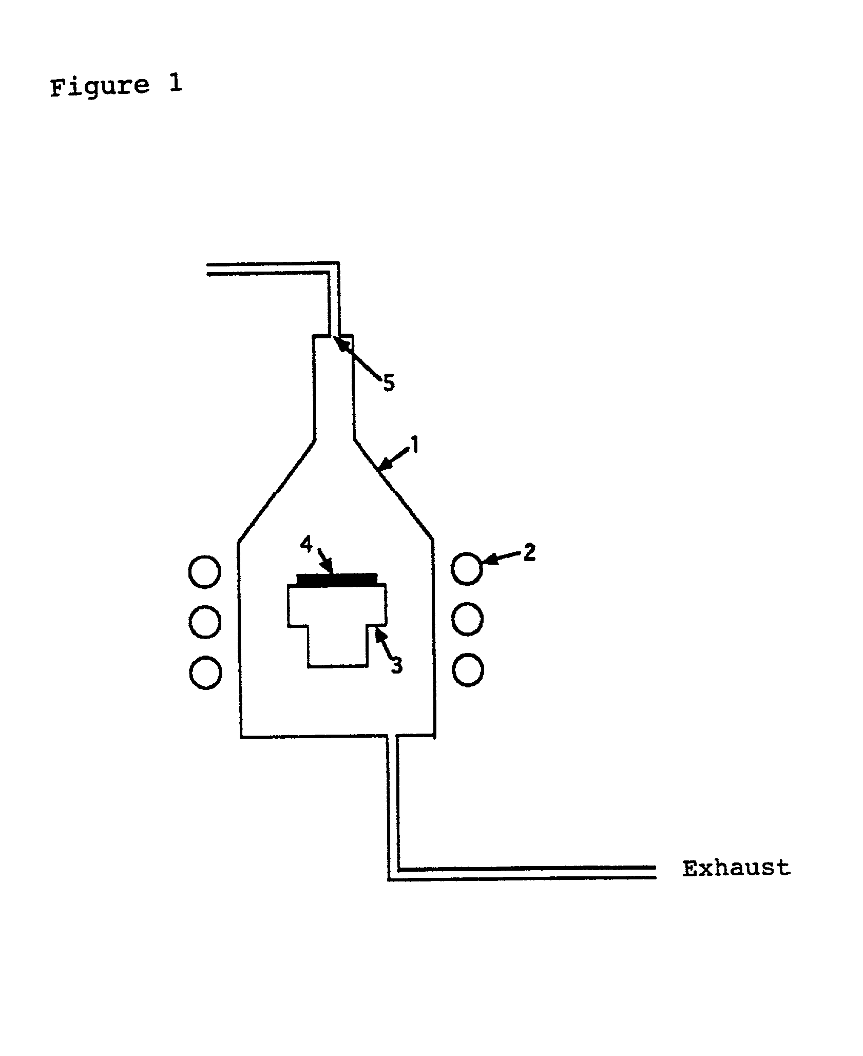
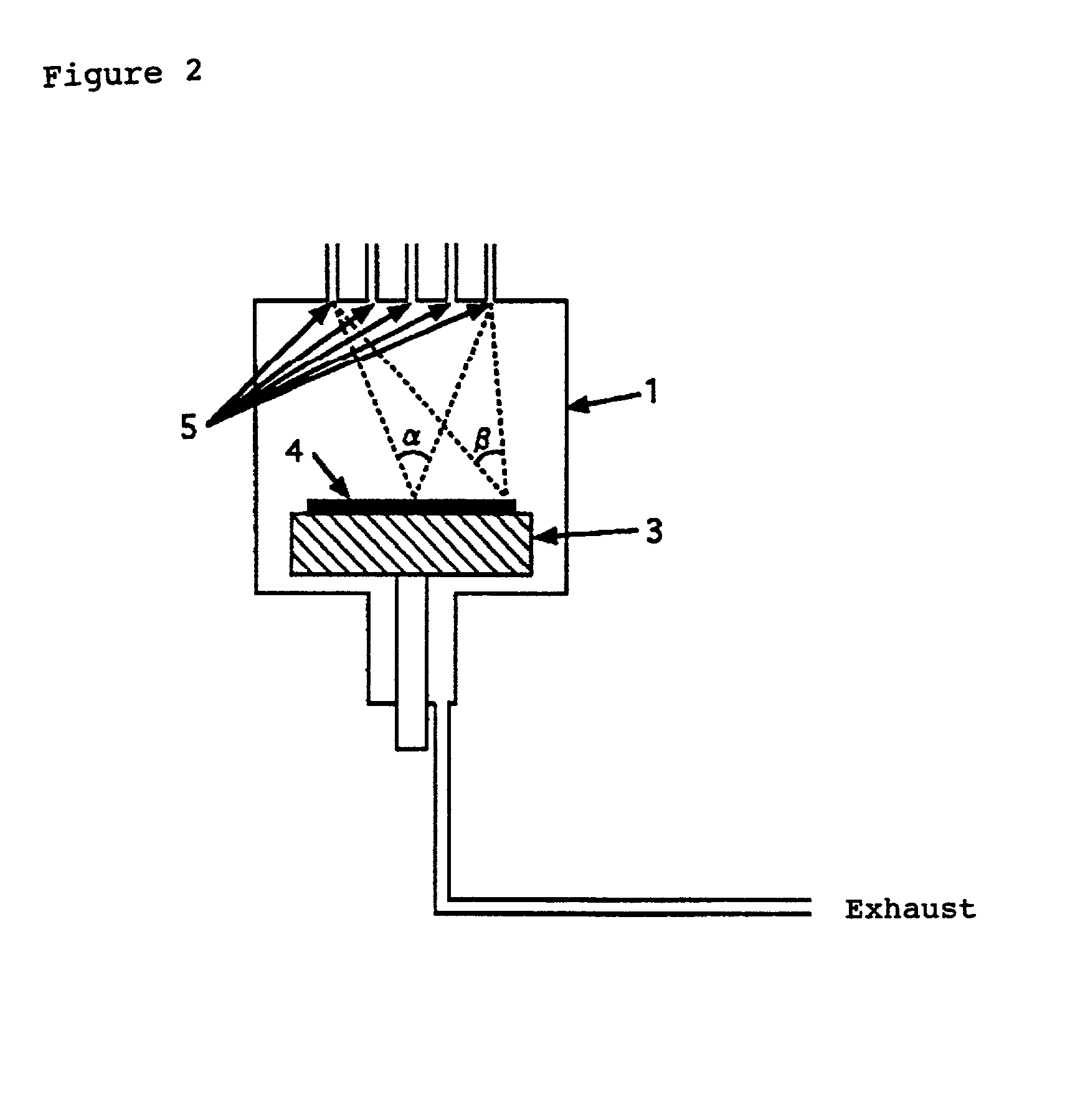

Image

  • Method of manufacturing group iii-v compound semiconductor
  • Method of manufacturing group iii-v compound semiconductor
  • Method of manufacturing group iii-v compound semiconductor

Examples


first example to

Compare

[0048] A sample was manufactured in the same manner as in the first embodiment, except for points that hydrogen gas was used as the carrier gas through the entire steps and that the supply of NH.sub.3 was stopped when the temperature of the susceptor was reduced to 600.degree. C.. Despite the effort to evaluate the sample in the same manner as in the first embodiment, it was impossible to evaluate the conductivity because of a high resistance.

second example to

Compare

[0049] A laminated structure consisting of non-doped GaN and Mg-doped GaN was manufactured in the same manner as in the first embodiment, except for points that hydrogen was added 50 SCCM during cooling down of crystal after growing the crystal. Carrier concentration of the sample was 3.times.10.sup.14 cm.sup.-3 when evaluated in the same manner as in the first embodiment.

second embodiment

[0050] After growing non-doped GaN to a thickness of 3 .mu.m using hydrogen as the carrier gas, supply of TMG was stopped, the carrier gas was changed to nitrogen, and the substrate was cooled down to a temperature of 800.degree. C., as in the first embodiment. Next, using TEG, TMI and TEA as materials, In.sub.0.l5Ga.sub.0.85N was grown to a thickness of 50.ANG. and Ga.sub.O.8Al.sub.0.2N was grown to a thickness of 300.ANG.. Further, the temperature of the substrate was increased to 1,100.degree. C. while supplying only nitrogen, i.e., the carrier gas, and ammonia, so as to grow Mg-doped GaN to a thickness of 5,OOO.ANG., in the same manner as in the first embodiment. After growing Mg-doped GaN, the substrate was cooled down and taken out as in the first embodiment except for the point that the supply of NH.sub.3 was stopped when the temperature of the susceptor was reduced to 600.degree. C., and the carrier concentration was measured. Measurement showed that the conductivity was p-t...


PUM


Abstract

The present invention provides for a method of manufacturing a Group III-V compound semiconductor, which grows a nitrogen-contained Group III-V compound semiconductor of the p-type conductivity, without performing any particular post-processing after growing the compound semiconductor, and which prevents a deterioration in the yield of manufacturing light emitting elements due to post-processing. [1] A method of manufacturing a Group III-V compound semiconductor which contains p-type impurities and which is expressed by a general formula InxGayAlzN (0>=x>=1,0>=z>=1, x+y+z=1), by thermal decomposition vapor phase method using metalorganics, the method being characterized in that carrier gas is inert gas in which the concentration of hydrogen is 0.5 % or smaller in capacity. [2] A method of manufacturing a Group III-V compound semiconductor which contains p-type impurities and which is expressed by a general formula InxGayAlzN (0>=x>=1, 0>=y>=1,0>=1, x+y+z=1), by thermal decomposition vapor phase method using metalorganics, the method being characterized in that after etching within a reaction furnace using at least one compound which is selected from a compound group consisting of compounds of halogenated hydrogen, compounds of halogen and Group V elements and compounds of halogen, hydrogen and Group V elements, inert gas in which the concentration of hydrogen is 0.5% or smaller in capacity is used as carrier gas.

Description

[0001] 1. Field of the Invention[0002] The present invention is related to a method of manufacturing a Group III-V compound semiconductor by thermal decomposition vapor phase method using metalorganics.[0003] 2. Description of the Background Art[0004] Since Group III-V compound semiconductors which are expressed by a general formula In.sub.xGa.sub.yAl.sub.zN (0.gtoreq.x.gtoreq.1, 0.gtoreq.z.gtoreq.1, x+y+z=1) have a band gap which can be controlled by a composition of Group III elements, Group III-V compound semiconductors can be used as a light emitting element which emits light ranging from the visible range to the ultraviolet range. In addition, since Group III-V compound semiconductors have a band structure of the direct transition type, using a Group III-V compound semiconductor, it is possible to obtain a light emitting element which has a high luminescence efficiency. Group III-V compound semiconductors in which the concentration of In is 10% or more, in particular, are impor...

Claims


Application Information

Patent Timeline
IPC IPC(8): C30B23/00C30B25/02C30B29/40H01L21/205H01L21/3205H01L21/4763
CPCC30B25/02C30B29/40Y10S438/93H01L21/0242H01L21/02661H01L21/0254H01L21/02579H01L21/0262H01L21/02458
Inventor IYECHIKA, YASUSHIONO, YOSHINOBUTAKADA, TOMOYUKI
Owner SUMITOMO CHEM CO LTD
Learn More