Clock controlling method and clock control circuit

a control circuit and clock technology, applied in the direction of generating/distributing signals, pulse techniques, instruments, etc., can solve the problems of difficult to generate multiplexed signals phase-synchronized with the external clock received, time-consuming lock process, and difficult to output a signal synchronization

Inactive Publication Date: 2002-05-16
RENESAS ELECTRONICS CORP
View PDF9 Cites 24 Cited by
  • Summary
  • Abstract
  • Description
  • Claims
  • Application Information

AI Technical Summary

Benefits of technology

0031] It is another object of the present invention to provide a novel clock control circuit for generating multi-phase clocks having equal clock intervals and a frequency multiplie...

Problems solved by technology

In the above-described clock control circuit, employing the PLL, in which an oscillation output signal from the voltage controlled oscillator (VCO) and the input signal (reference signal) are controlled so as to match in phases to each other, a lock process is time consuming, and it is difficult to output a signal synchronized with the oncoming input clock immediately from the clock cycle next following the oncoming input clock in case of the PLL being in an unlocked state or in case of no input clock(reference signal) being provided to the PLL from the perspective of the circui...

Method used


Image

  • Clock controlling method and clock control circuit
  • Clock controlling method and clock control circuit
  • Clock controlling method and clock control circuit

Examples


first embodiment

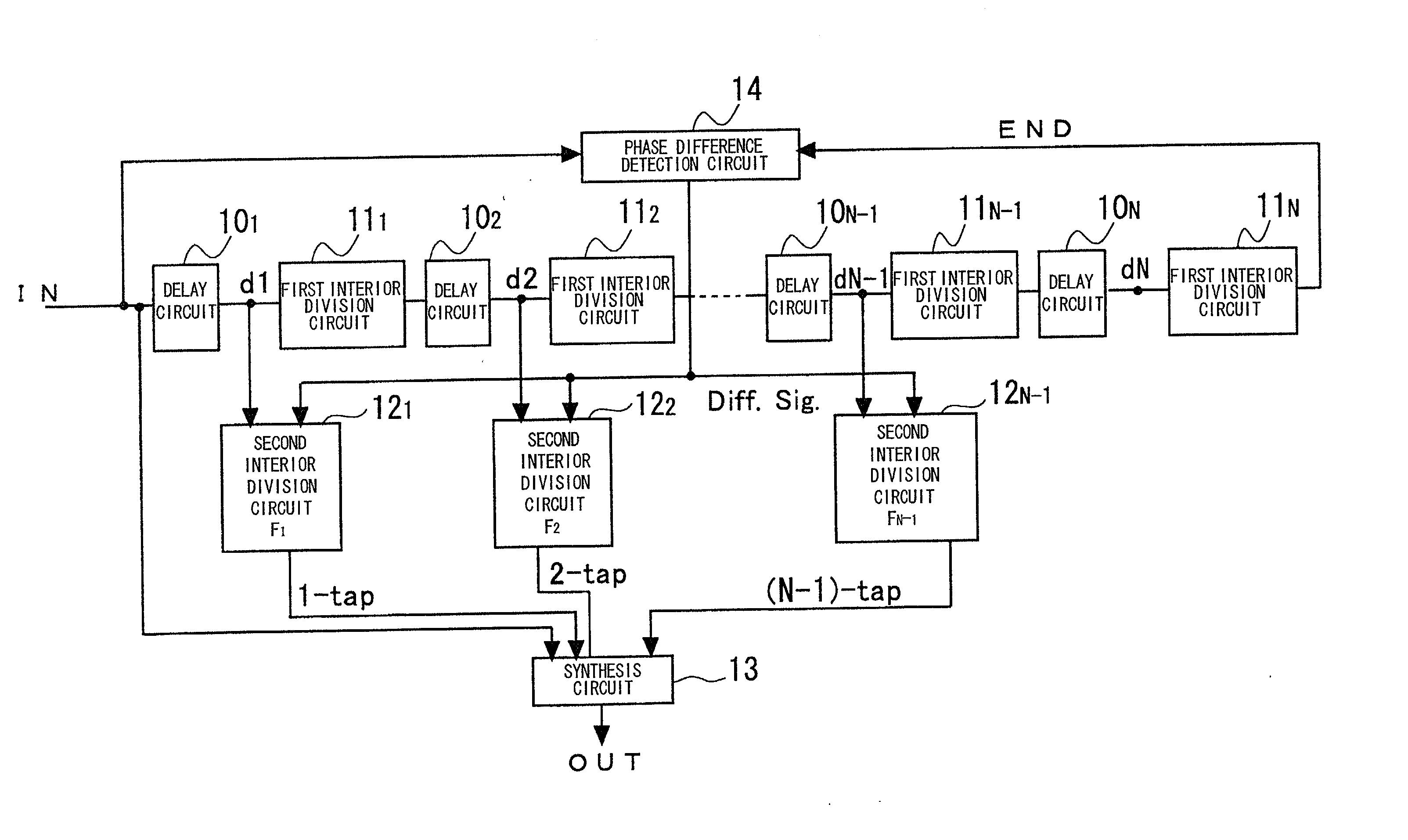
[0139] FIG. 5 shows an illustrative structure of the first interior division circuit 11 in the present invention. In FIG. 5, the first interior division circuit 11 is basically comprised of a timing difference division circuit shown in FIG. 14, and is made up of a p-channel MOS transistor MP01 which is connected across a power supply VDD and an internal node N1, a logical OR circuit OR1 which receives signals from two input terminals IN1, IN2 and has its output terminal connected to the gate of the p-channel MOS transistor MP01 to be adapted to turn on the p-channel MOS transistor MP01 when the input signals fed to the two input terminals IN1 and IN2 in common are low, an inverter INV03 which has its input terminal connected to the internal node N1, m pieces of n-channel MOS transistors which are connected across the internal node N1 and the ground and have the gates fed in common with the input signal supplied to the input terminal IN1, and N-m pieces of n-channel MOS transistors w...

second embodiment

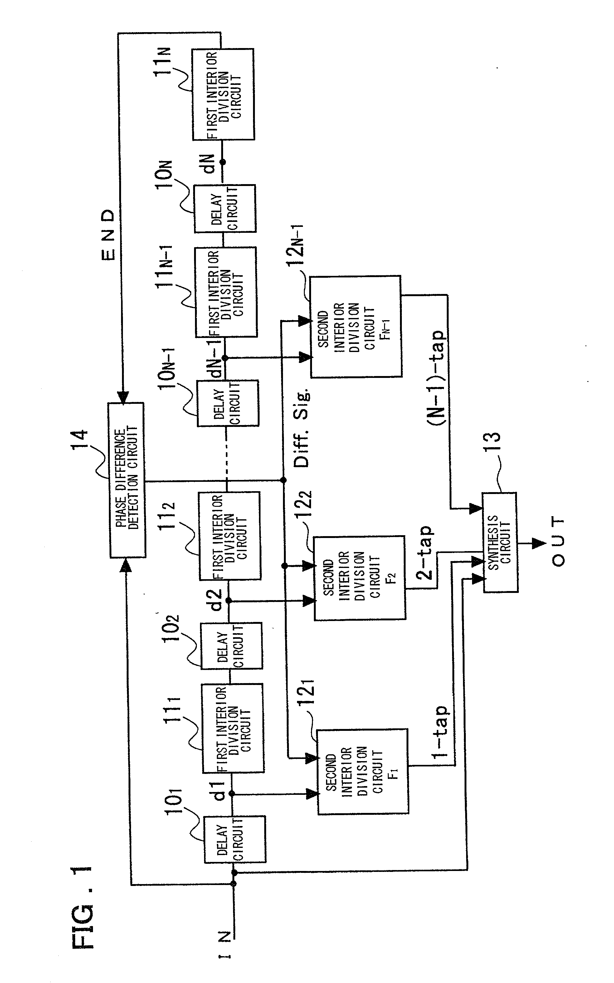
[0177] The second interior division circuit 12 is configured similarly to the second interior division circuit 12 of the above described second embodiment which is explained with a reference to FIGS. 6 and 9. However, the setting of the magnitude relation between the delay time in the number 1 to number N second interior division circuits 12.sub.1 to 12.sub.N differs from that of the previous embodiment. That is, in the present embodiment, the delay time is increased by steps of T / N sequentially in the order of the number 1 second interior division circuit 12.sub.1 to the number N second interior division circuit 12.sub.N, with the number N second interior division circuit 12.sub.N having the maximum delay time.

[0178] Referring to FIG. 6, the number n second interior division circuit 12.sub.n includes a first second switch (p-channel MOS transistor MP1) for controlling on and off of a charging path to the capacitor C provided in the circuit, a plural number of second switches (n-cha...

fifth embodiment

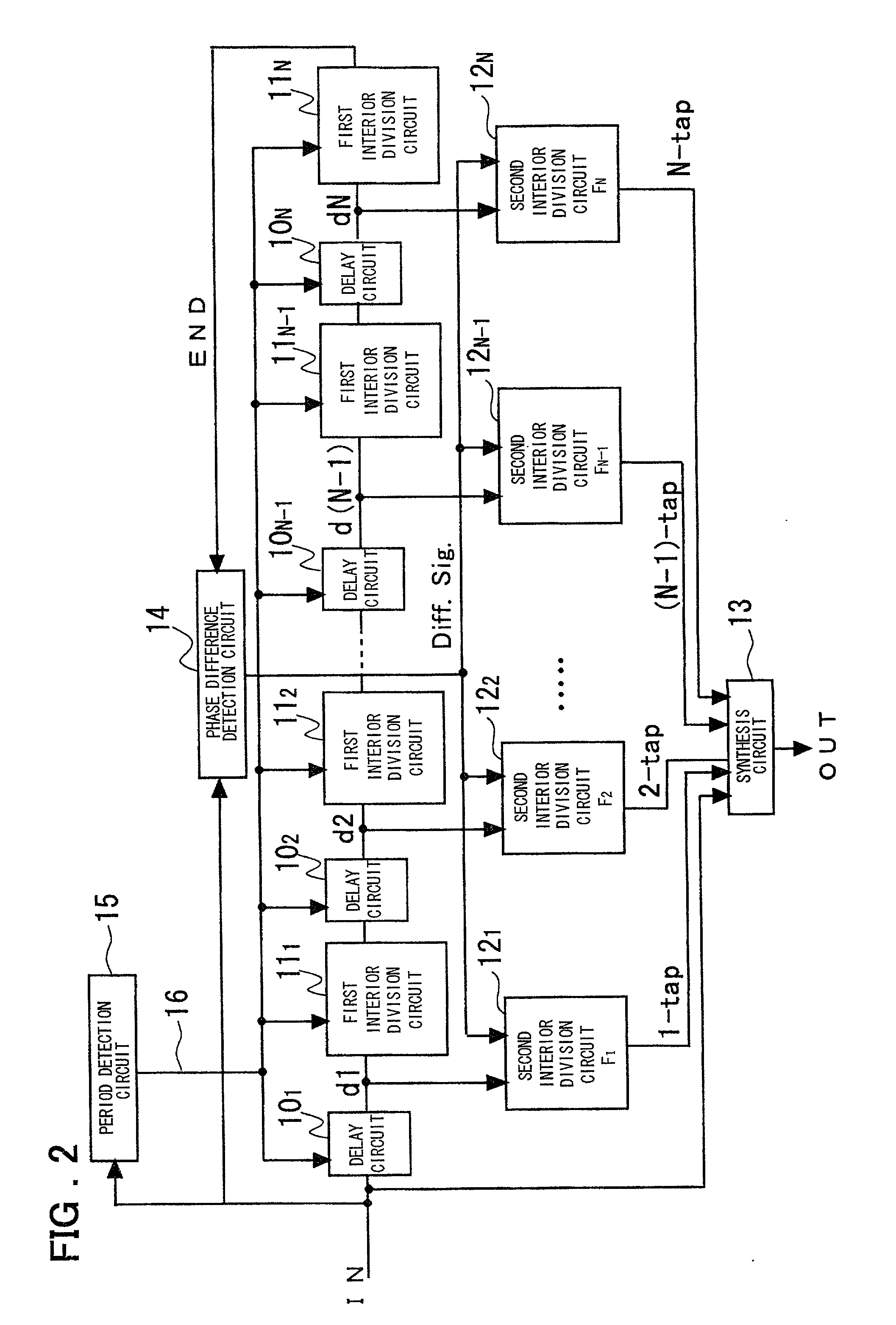
[0266] A further embodiment of the present invention is explained. FIG. 20 shows the structure of this modified embodiment suitable for high-speed clock transmission. While in the embodiment shown in FIG. 17, an unbalanced clock transmission system is adopted, the present fifth embodiment of the present invention, shown in FIG. 20, a balanced clock transmission path is adopted and there are provided 2N delay circuits 10.sub.1 to 10.sub.2N and 2N delay circuits 10.sub.B1 to 10.sub.BN for each of the clock CLK and complementary clock having a reversed in phase (out of phase by 180.degree. (.pi.)) with respect to the clock CLK, and interior division circuits 12.sub.0 to 12.sub.N and 12.sub.B0 to 12.sub.BN, for the respective clocks. The interior division circuits 12.sub.0 to 12.sub.N and 12.sub.B0 to 12.sub.BN generate multi-phase clocks corresponding to 2N equal division of the clock period tCK. The delay circuits 10.sub.1 to 10.sub.2N and the delay circuits 10.sub.B1 to 10.sub.B2N ma...


PUM


Abstract

A novel clock control circuit and method in which phase synchronization with respect to an external clock can be realized without recourse to the external clocks. A clock controlling circuit includes a delay circuit sequence comprised of N stages of units each made up of a first delay circuit 10 and a first interior division circuit 11 for delaying the output signal of the first delay circuit, and a phase difference detection circuit 14 for detecting the clock period and the delay time difference of the delay circuit sequence from the input clock IN and a clock END output by the delay circuit sequence as a phase difference of the two signals. A plural number of second interior division circuits 12, fed with an output signal of the first delay circuit, delays a transition edge of an output signal of the first delay circuit by t2-nxT/N to output the delayed signal. The second interior division circuit outputs a signal which makes transition at a timing delayed nxtCK/N as from the start time point of the clock cycle. A synthesis circuit 13 generates a frequency multiplied clock signal which is obtained on equal division of the clock period tCK of the input clock from the input clock IN and the number 1 to numberN-1 third delays circuit.

Description

[0001] This invention relates to a clock controlling method and a clock control circuit. More particularly, it relates to a clock controlling method and a clock control circuit convenient for generating a clock signal having a multiplied frequency of an external clock and being synchronized with the external clock.[0002] Recently, with an increasing size of circuits that can be integrated on one chip and with an increasing operating frequency, a clock control circuit has come to be used for controlling the phase and frequency of clock inside and outside a chip of a semiconductor integrated circuit including a synchronization circuit operating on a clock signal supplied to the circuit.[0003] As a clock control circuit, a feedback type circuit, such as a PLL (phase locked loop) or a DLL (delay synchronization loop), has so far been used. Of these, the PLL circuit is made up of a phase comparator circuit receiving a reference clock signal as an input, a charge pump for charging and dis...

Claims


Application Information

Patent Timeline
IPC IPC(8): G06F1/08G06F1/06G06F1/10G06F7/68H03K5/00H03K5/08H03K5/13H03K5/15H03K7/08H03L7/00
CPCG06F1/10G06F7/68H03K5/082H03L7/00H03K5/1504H03K2005/00065H03K2005/00071H03K5/13H03K7/08
Inventor SAEKI, TAKANORI
Owner RENESAS ELECTRONICS CORP
Why Eureka
Try Eureka