

Lateral polysilicon pin diode and method for so fabricating
a technology of polysilicon pin diodes and lateral pin diodes, which is applied in the direction of photovoltaic energy generation, electrical equipment, semiconductor devices, etc., can solve the problems of insufficient thickness of materials and a great deal of charge storage, and achieve the effect of extending the charge storage area
- Summary
- Abstract
- Description
- Claims
- Application Information
AI Technical Summary
Benefits of technology
Problems solved by technology
Method used
Image

Examples
first embodiment
[0028]
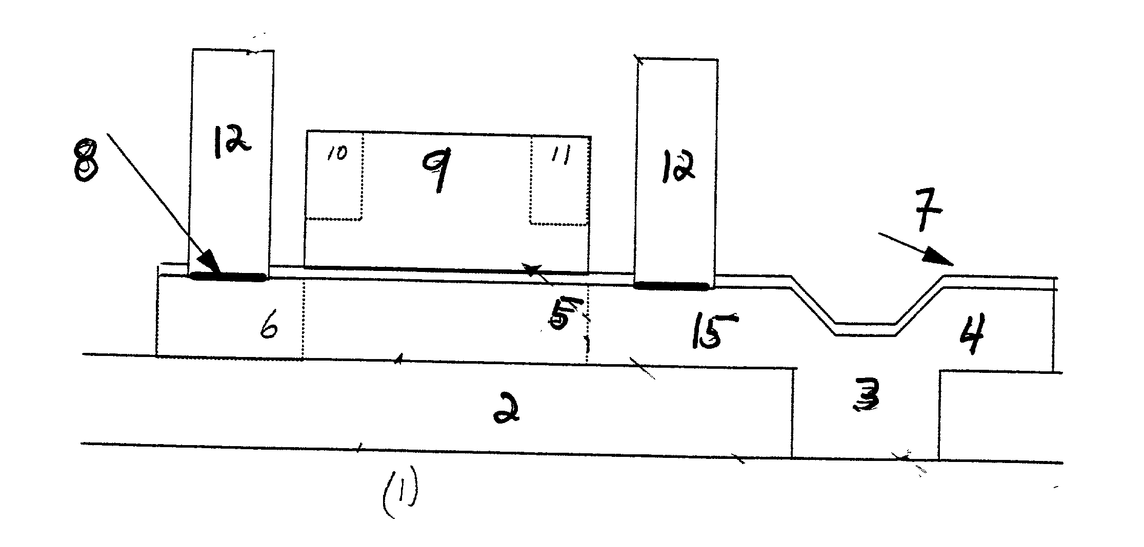
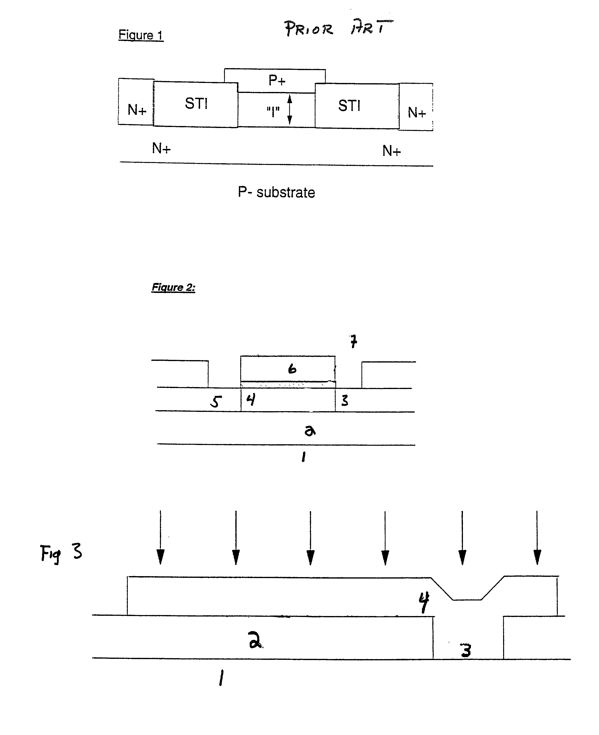
[0029] Referring now to FIG. 2. The first version comes for free in an epitaxial-base bipolar process such as silicon-germanium BICMOS technology. The semiconductor substrate 1 is standard as is the about 2800 .ANG. oxide layer 2 provided on a top surface. The base polysilicon is used to form the body of the PIN diode and is appropriately masked and doped to yield N+ 3, intrinsic (I) 4, and P+ 5 regions. Emitter-base passivation 7 is used to form the passivating layer for the polysilicon, to help reduce the surface recombination by using a high-quality thermal oxide interface. The emitter polysilicon 6 forms a masking layer that prevents future implants from getting into the body of the diode. On this polysilicon layer, the edges of the masks for P+ and N+ implants on either side of the PIN diode body are defined. Prior art PIN diodes are restricted to I-regions of about 0.5 .ANG. by the thickness of the epitaxial layer in which it is formed. By arranging the I-region laterall...
second embodiment
[0031]
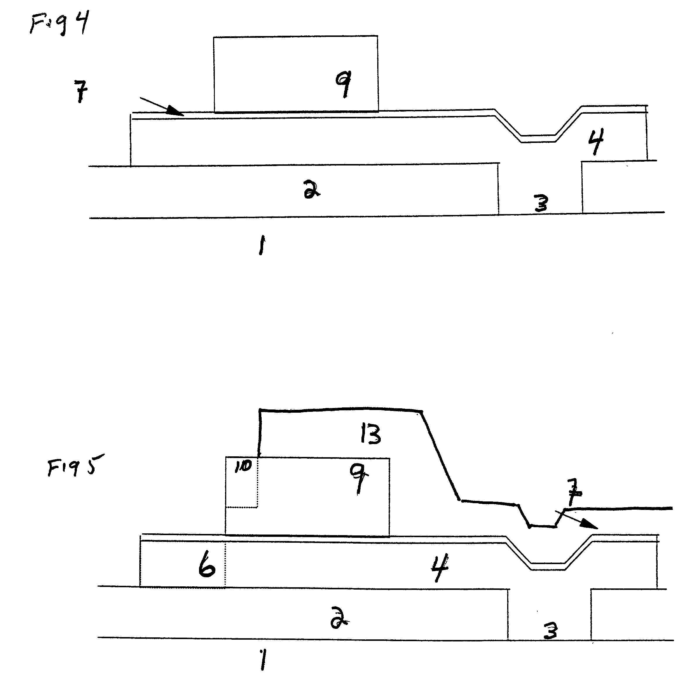
[0032] In an alternative embodiment, an extra mask can be used to open a region of the base polysilicon over the single crystal base, through the emitter-base passivation. The amorphous silicon layer used for the passivation can then be deposited and annealed. This results in epitaxial lateral growth of the amorphous silicon from the seed area in the single crystal base. This results in a single crystal structure which has reduced recombination current. In a fashion similar to the first embodiment, a passivation and masking layer can be formed on top, and the P+ and N+ implants can be defined into opposite ends of the diode body.
[0033] Turning now to FIG. 3, a sequence of steps for fabrication of a second embodiment is recited. This recitation refers to a preferred embodiment wherein the substrate is silicon. Therefore, silicon-specific means, such as silicon-specific isolations and process steps are recited. However, it is to be understood that the present invention is capabl...
PUM
 Abstract
Description
Claims
Application Information