Method of forming germanium doped polycrystalline silicon gate of MOS transistor and method of forming CMOS transistor device using the same

a technology of germanium doped polycrystalline silicon and mos transistor, which is applied in the direction of transistors, semiconductor devices, electrical devices, etc., can solve the problems of reducing drain current, reducing gate depletion, and so difficult to control the process

Inactive Publication Date: 2002-06-13
SAMSUNG ELECTRONICS CO LTD
View PDF0 Cites 21 Cited by
  • Summary
  • Abstract
  • Description
  • Claims
  • Application Information

AI Technical Summary

Benefits of technology

[0014] Thus, it is an object of the present invention to provide a method of forming polycrystalline silicon germanium gate electrode by which a considerable amount of germanium can be doped effectively and to provide a method of forming CMOS transistor by using the same.
[0015] It is another object of the present invention to provide a method of forming polycrystalline silicon germanium gate electrode by which the doping concentration of germanium can be controlled with exactness and to provide a method of forming CMOS transistor by using the same.
[0016] It is also one object of the present invention to provide a method of forming CMOS transistor by which boron concentration can be sustained enough only in polycrystalline silicon gate electrode of PMOS transistor region.
[0019] In the present invention, the process of plasma doping of germanium may have the following steps: making a germanium containing plasma by supplying germanium source to a process chamber which has plasma enhancing devices, enhancing bias electric potential to the substrate for the formed germanium plasma to be accelerated to the substrate and to be injected into the substrate, more strictly to polycrystalline silicon layer revealed.
[0021] In the plasma doping of the present invention, because only the germanium source is supplied, the total amount of supply and the concentration of germanium in the gate can be more stably controlled compared to CVD doping method in which the germanium source gas mixed with SiH4 gas is supplied. And, because the germanium source is supplied directly to the process chamber to form germanium plasma and the germanium plasma is directly accelerated to substrate, doping with high dose ranging from 1E16 to 1E17 ions / square centimeter and forming of polycrystalline silicon germanium layer of over 10% germanium concentration can be executed in a practical process.

Problems solved by technology

However, Boron may cause gate depletion.
And, the gate depletion lowers conductivity of gate and increases the effective thickness of gate insulation layer causing problems such as decrease in drain current.
But, in this method, controlling the process is so difficult that it is hard to secure uniformity and reliability of germanium concentration.
However, germanium, for example, germanium of 10% or more in the gate electrode of NMOS transistor lowers the solubility of polycrystalline silicon gate to N type impurities and lowers the capacitance of gate.
This causes the degradation of transistor in CMOS devices.
But, to obtain germanium of 20.about.30 weight % in polycrystalline silicon germanium gate, an amount of 1E16 ions / square centimeter or more dose corresponding to ion implantation continued for 10 or more hours are needed, which means the process does not have actual productivity.

Method used


Image

  • Method of forming germanium doped polycrystalline silicon gate of MOS transistor and method of forming CMOS transistor device using the same
  • Method of forming germanium doped polycrystalline silicon gate of MOS transistor and method of forming CMOS transistor device using the same
  • Method of forming germanium doped polycrystalline silicon gate of MOS transistor and method of forming CMOS transistor device using the same

Examples


embodiment 1

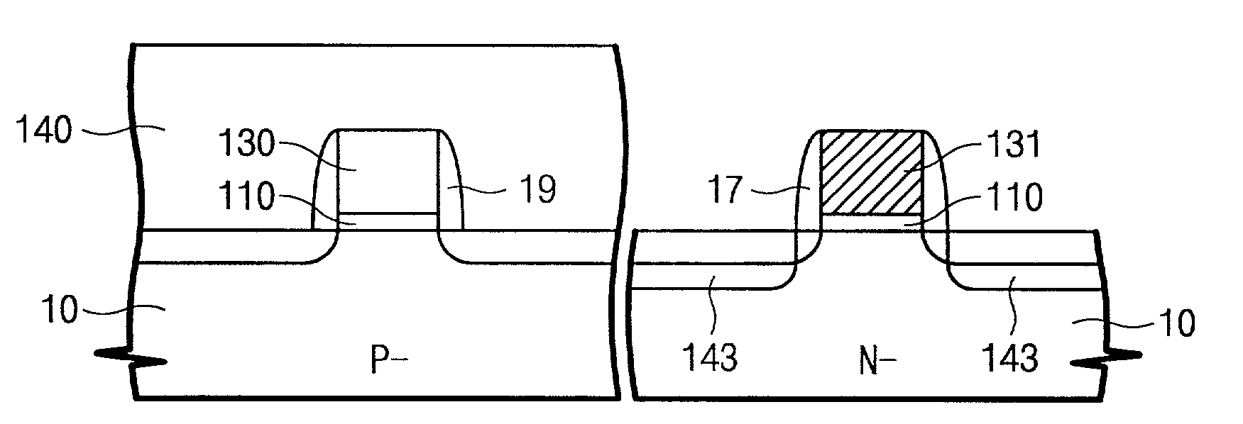
[0032] In this embodiment, CMOS transistor is explained and PMOS transistor part and NMOS transistor part of the CMOS transistor are individually explained in some step of the present invention.

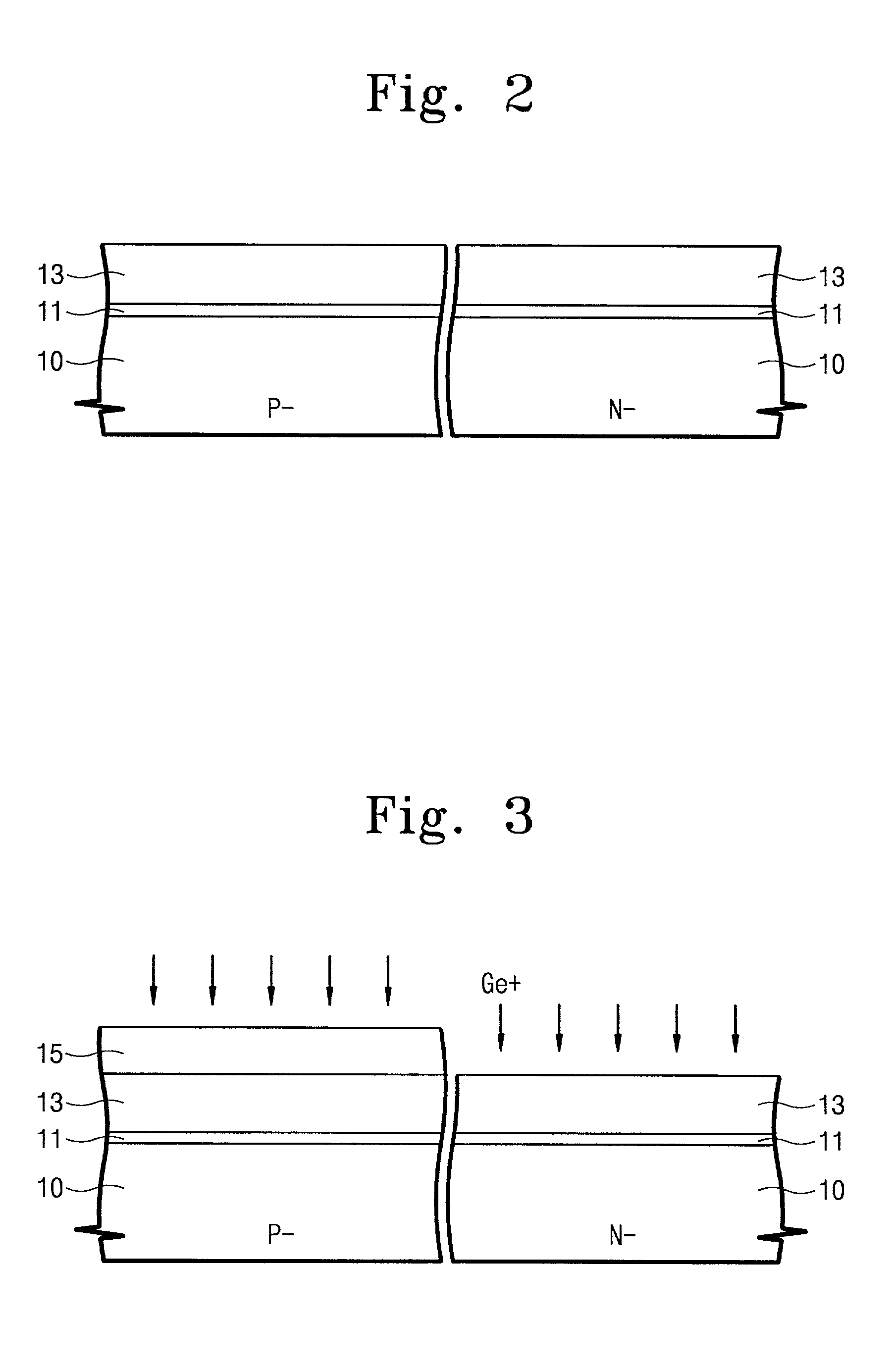
[0033] Referring to FIG. 2, a gate insulation layer 11 made of silicon oxide is formed on the substrate 10 by oxidizing the surface silicon of the substrate 10. A pure polycrystalline silicon layer 13 of 1000.about.2000 angstroms is formed on the gate insulation layer 11 by CVD (Chemical Vapor Deposition). Before forming a gate insulation layer, although not shown, an N type substrate having P well is supplied and device isolation is performed in the substrate.

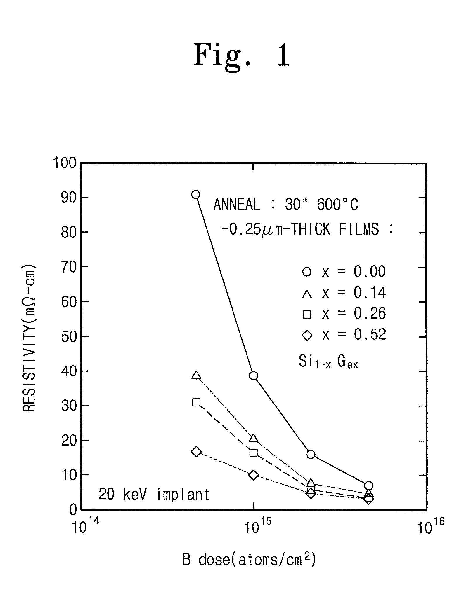
[0034] Referring to FIG. 3, doping mask 15 to cover NMOS transistor region is formed with photoresist by general photolithography process. Then, germanium plasma is made by supplying germanium-contained source gas into process chamber supplied with plasma enhancing apparatus. For this process of making germanium plasma, the atmospheric ...

embodiment 2

[0040] Referring to FIG. 7, a gate insulation layer 11 made of silicon oxide is formed on the substrate 10 by oxidizing the surface silicon of the substrate 10. A pure polycrystalline silicon layer 23 of 200.about.1000 angstroms is formed on the gate insulation layer 11 by CVD (Chemical Vapor Deposition). Before forming gate insulation layer, an N type substrate having P well is supplied and device isolation is performed in the substrate.

[0041] Referring to FIG. 8, doping mask 15 to cover NMOS transistor region is formed with photoresist layer by general photolithography process. Then, germanium plasma is made by supplying germanium-contained source gas into process chamber and enhancing electric field varying with radio frequency.

[0042] Conditions and arrays of procedure adapted in Embodiment 1 can also be applied to this embodiment. And resultantly, dose of 1E15 to 1E17 ions / square centimeter is doped to form several ten angstroms or several hundred angstroms of polycrystalline si...


PUM

PropertyMeasurementUnit
thicknessaaaaaaaaaa
thicknessaaaaaaaaaa
thicknessaaaaaaaaaa

Abstract

A method of forming polycrystalline silicon germanium gate electrode is disclosed. The method include the steps of forming gate insulation layer on a substrate, forming a polycrystalline silicon layer on the gate insulation layer and making a plasma doping of germanium to the polycrystalline silicon layer. Generally, boron is doped to the polycrystalline silicon after the step of the plasma doping of germanium. The process of plasma doping of germanium comprises the step of forming germanium contained plasma and enhancing bias electric potential to substrate for the formulated germanium plasma to be accelerated and injected to the polycrystalline silicon layer revealed. If the present invention is applied to CMOS transistor device, doping mask for the germanium plasma doping can be used.

Description

[0001] This application relies for priority upon Korean Patent Application No. 2000-75643, filed on Dec. 12, 2000, the contents of which are herein incorporated by reference in their entirety.FIELD OF THE INVENTION[0002] The present invention is related to method of forming semiconductor devices and, more particularly, to method of forming gate electrode of MOS transistor made of polycrystalline silicon-germanium and method of forming CMOS transistor device using the same.BACKGROUND OF THE INVENTION[0003] PMOS transistors can be used having no relation to NMOS transistor in a semiconductor device. But, usually, PMOS transistors are used with NMOS transistor in CMOS type semiconductor devices. In a CMOS type semiconductor device, PMOS transistors and NMOS transistors are connected with each other and work together complementarily. Resultantly, the operation speed and efficiency of device can be improved and CMOS transistor has characteristics similar to those of bipolar type transist...

Claims


Application Information

Patent Timeline
Patent Type & Authority Applications(United States)
IPC IPC(8): H01L21/265H01L21/28H01L21/3215H01L21/8238H01L21/336H01L27/092H01L29/78
CPCH01L21/2807H01L21/32155H01L21/823842Y10S438/933H01L21/18
Inventor HA, JUNG-MINPARK, JUNG-WOO
Owner SAMSUNG ELECTRONICS CO LTD
Why Eureka
Try Eureka