N-channel metal oxide semiconductor (NMOS) driver circuit and method of making same

a driver circuit and metal oxide semiconductor technology, applied in semiconductor devices, semiconductor/solid-state device details, electrical apparatus, etc., can solve the problems of substantially worse short-channel effect, channel pfet, or nfet, and is generally more expensive than a single-work function-gate process

Inactive Publication Date: 2002-07-11
IBM CORP
View PDF0 Cites 2 Cited by
  • Summary
  • Abstract
  • Description
  • Claims
  • Application Information

AI Technical Summary

Problems solved by technology

Since a dual-workfunction-gate process requires extra mask steps and extra implant steps, it is generally more expensive than a single-work function-gate process.
However, when the single-work function-gate process is used (e.g., N+ polysilicon gate only), the PFETs typically are buried channel PFETs, which have a substantially worse short-channel effect as compared with surface channel PFETs, or NFETs.
When the threshold voltage is below the designed target, excessive leakage current may occur even when the gate should supposedly be "OFF".
Buried channel PFETs also tend to be more susceptible to the "punchthrough effect".
When punchthrough occurs, the drain current will no longer be controlled by the gate voltage.
The loss of gate control can lead to circuit malfunction.
This not only leads to circuit area penalty, but also to performance degradation.
One of the limitations for the highest boosted WL voltage Vpp is the reliability of the buried channel PFET used in the WL driver region.
Carriers with high enough energy can overcome the barrier at the gate oxide interfa

Method used


Image

  • N-channel metal oxide semiconductor (NMOS) driver circuit and method of making same
  • N-channel metal oxide semiconductor (NMOS) driver circuit and method of making same
  • N-channel metal oxide semiconductor (NMOS) driver circuit and method of making same

Examples


Embodiment Construction

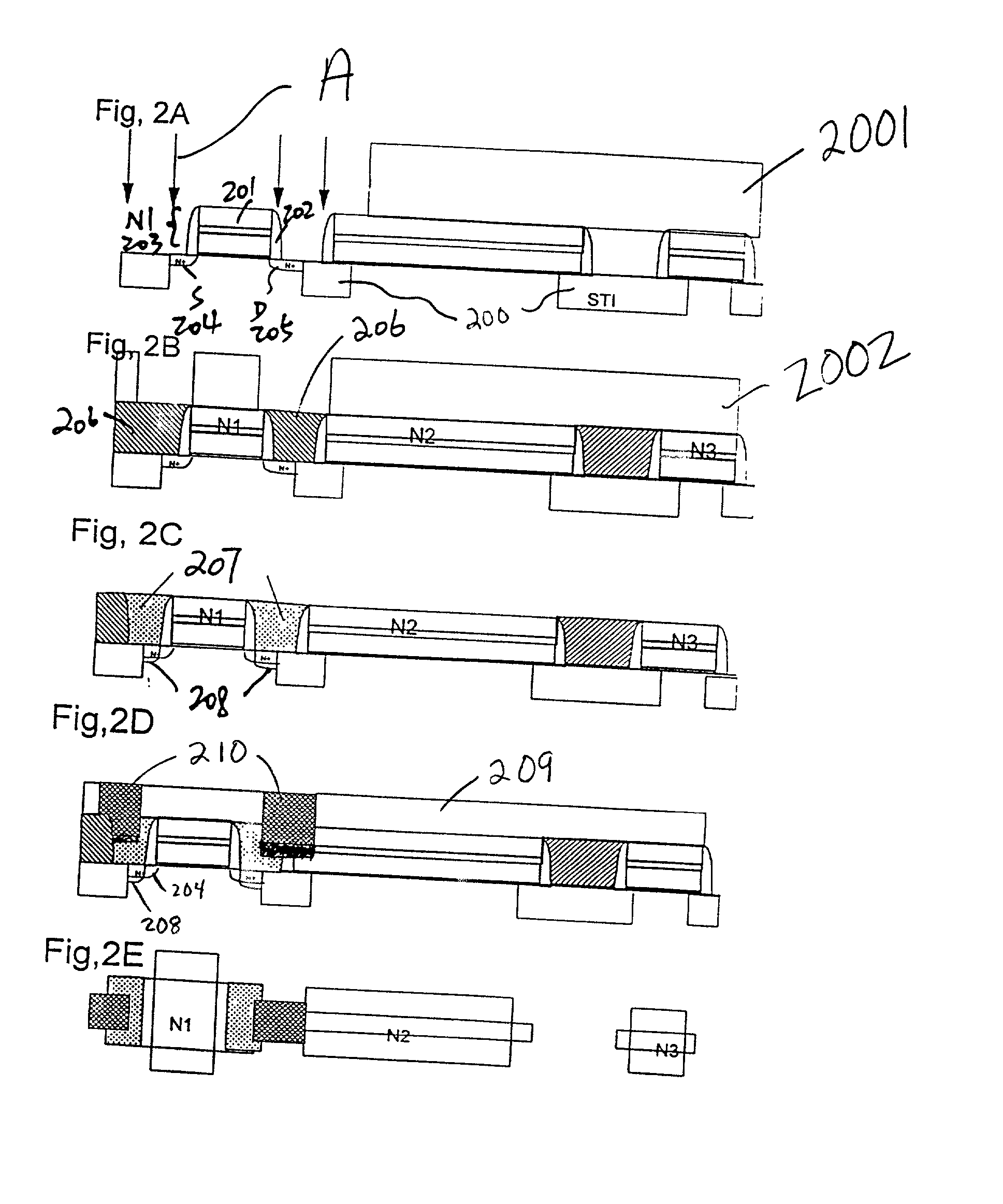
[0038] Referring now to the drawings, and more particularly to FIGS. 2A-5, an embodiment of the present invention will be described.

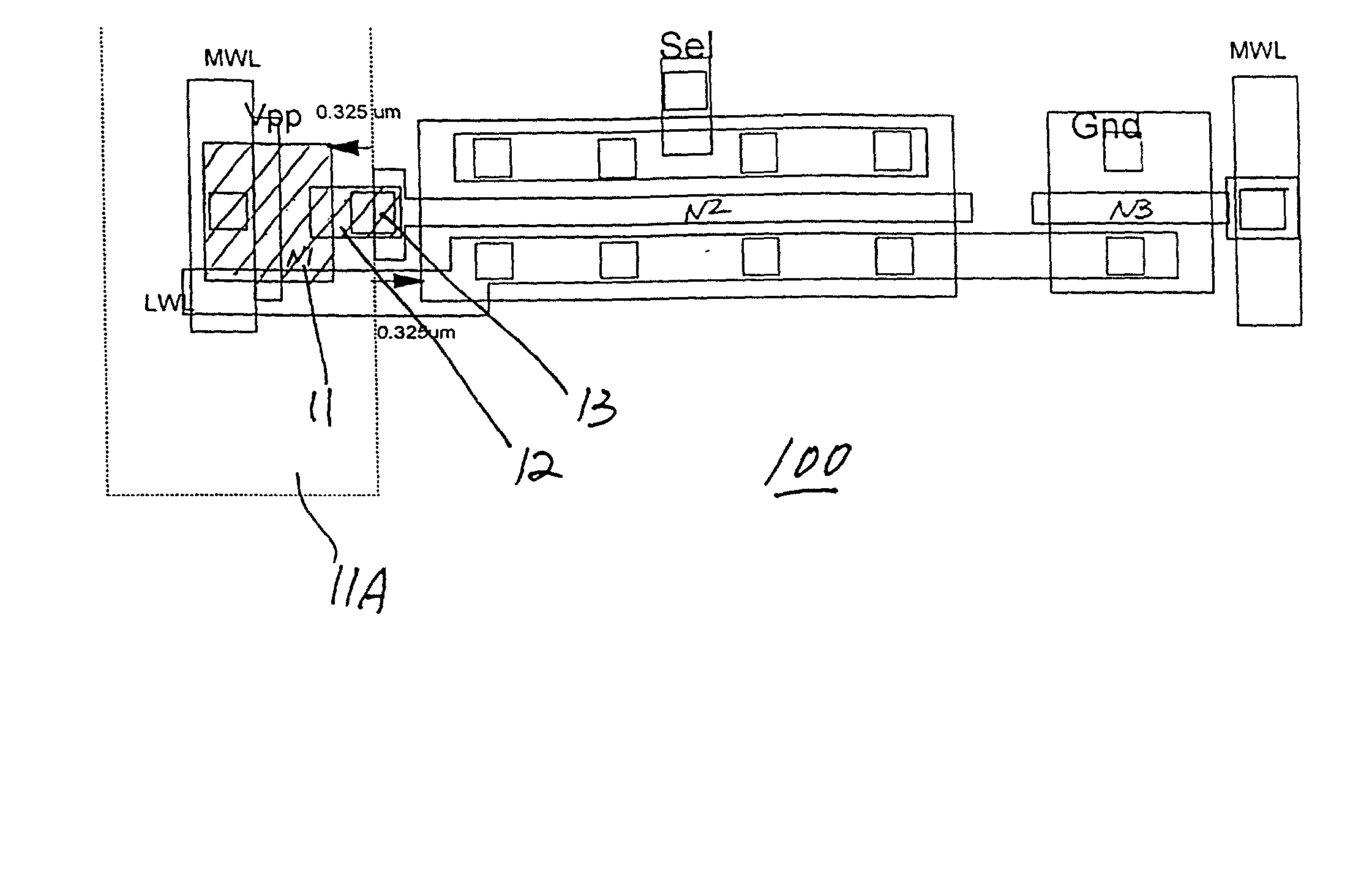
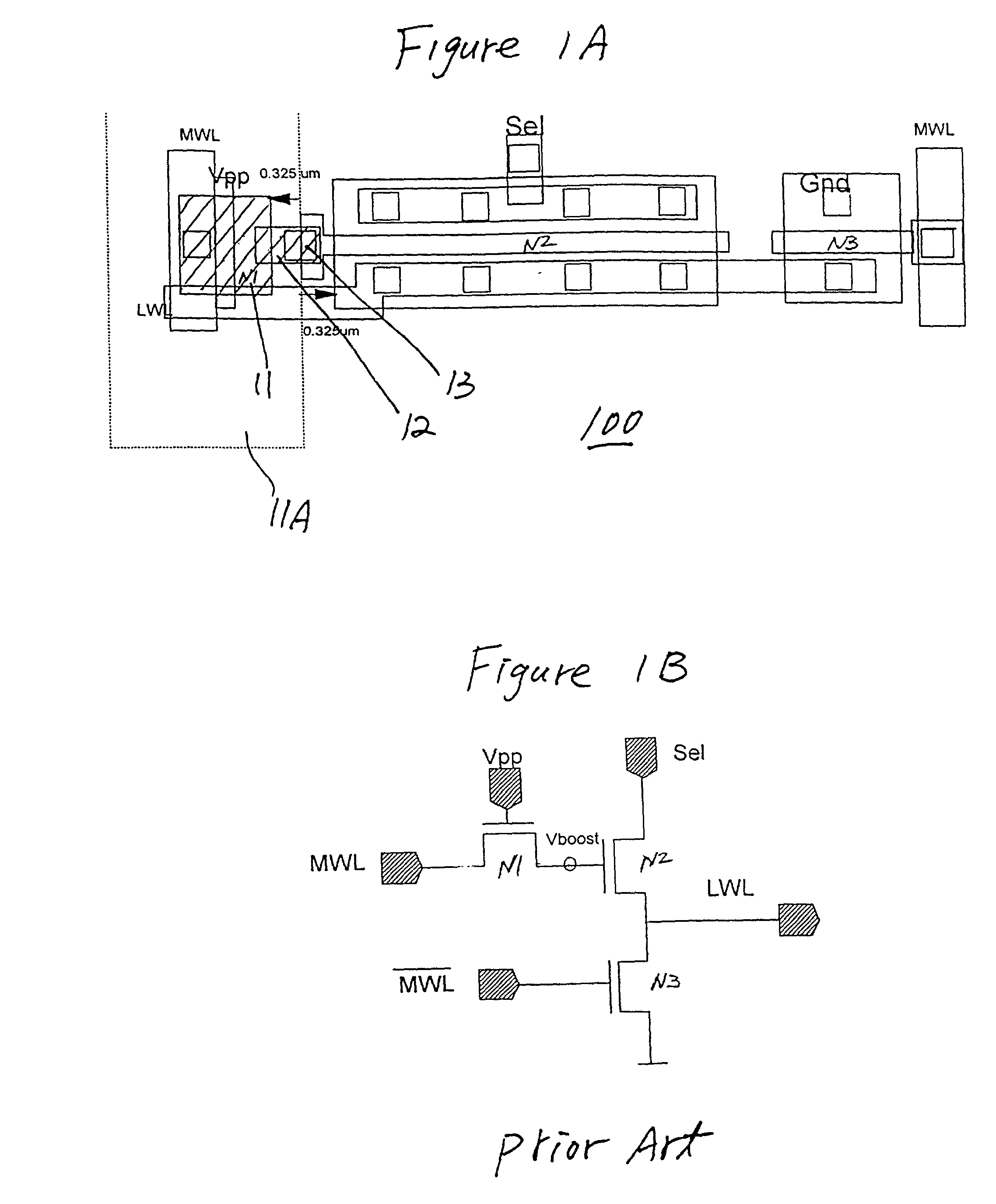
[0039] In FIG. 1A, a top view of an NMOS driver circuit 100 is shown. The shape of a contact bitline (CB) mask, or the cross-hatched area, for a boost device 11 (e.g., N1) is shown in FIG. 1A. The CB mask is for forming contacts and for driving in more dopant.

[0040] As a result, the boost device 11 will have XA implant, or a lower concentration N-type array implant, 11A and its serial resistance is reduced by the self-aligned CB diffusion. Arranging the device 11 close to the array allows it to be implanted by XA mask without increasing the support area, and thereby increases the density.

[0041] Through a CB extension 12, the CB contact 12 is formed in a self-aligned manner which abuts the gate of the pull-up NMOS device N2, as shown in FIG. 1A. The connection (e.g., joint) of the boost node to the gate is performed by a contact support (CS) 13, as shown...


PUM


Abstract

An N-channel metal oxide semiconductor (NMOS) driver circuit (and method for making the same), includes a boost gate stack formed on a substrate and having a source and drain formed by a low concentration N-type implantation, and an N-driver coupled to the boost gate stack.

Description

[0001] 1. Field of the Invention[0002] The present invention generally relates to an NMOS driver circuit, and a method of fabricating an NMOS driver circuit with improved performance and reliability.[0003] 2. Description of the Related Art[0004] An N-channel metal oxide semiconductor (NMOS) driver is known to have certain advantages as compared to conventional complementary oxide semiconductor (CMOS) drivers (e.g., such as P-channel field effect transistors (PFETs), N-channel field effect transistors (NFETS) and the like), such as smaller area, a switching performance gain, and less gate oxide stress.[0005] The NMOS driver has a smaller area compared to a CMOS driver based on similar performance. Such a smaller area results from the CMOS device (e.g., PFETs, NFETs, etc.) having a design width which is double that of the NFET device because of a difference in hole and electron mobility. The mobility of electrons, which are the conducting carriers for NFETs, is about two times that of...

Claims


Application Information

Patent Timeline
IPC IPC(8): H01L23/522H01L21/225H01L21/336H01L21/768H01L21/8234H01L21/8242H01L27/088H01L27/108
CPCH01L21/2251H01L21/76895H01L27/088H01L29/6659Y10S438/969H01L21/18
Inventor CLEVENGER, LAWRENCE A.DIVAKARUMI, RAMAHSU, LOUIS LU-CHENLI, YUJUN
Owner IBM CORP
Why Eureka
Try Eureka