Method for forming a deposited film by plasma chemical vapor deposition

a chemical vapor deposition and deposited film technology, applied in chemical vapor deposition coatings, coatings, electric discharge tubes, etc., can solve the problems of large area deposited film being inferior, difficult to form a large area deposited film stably and continuously, and foregoing problems relating to film properties

Inactive Publication Date: 2002-07-11
CANON KK
View PDF4 Cites 55 Cited by
  • Summary
  • Abstract
  • Description
  • Claims
  • Application Information

AI Technical Summary

Benefits of technology

[0015] According to the film-forming method of the present invention, it is possible to stably and efficiently form a high quality large area deposited film having a homogeneous property over the entire area thereof.

Problems solved by technology

But it is difficult to stably and continuously form a large area deposited film which is satisfactory in terms of the uniformity of the property even when such large-sized plasma CVD apparatus is used.
However, any of these methods tends to entail a problem in the case of forming a large area deposited film in that the resulting large area deposited film is apparently inferior to a small area deposited film formed by the foregoing plasma CVD apparatus which copes with a small film-forming area in terms of the uniformity of the property distribution and also in terms of the property as a whole.
That is, it was found out that the cause of the foregoing problems relating to the film property in the prior art is due to (i) inappropriateness of the proportion between precursors (which contribute to forming a deposited film) which are generated from a film-forming raw material gas (excluding H.sub.2 gas) and species generated from other raw material gas and (ii) inappropriateness of the ratio of the number of said precursors to that of hydrogen radicals generated.

Method used


Image

  • Method for forming a deposited film by plasma chemical vapor deposition
  • Method for forming a deposited film by plasma chemical vapor deposition
  • Method for forming a deposited film by plasma chemical vapor deposition

Examples


examples a1

[0121] Examples A1 to A4 are of the first aspect of the present invention, and Examples B1 to B4 are of the second aspect of the present invention.

example a1

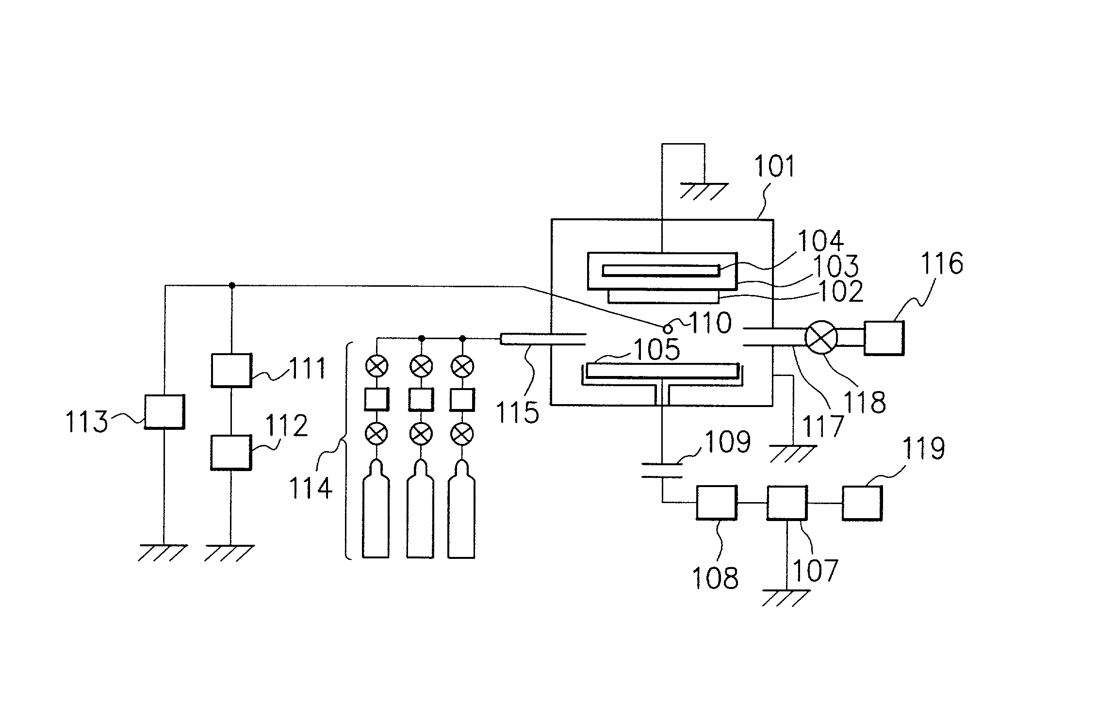
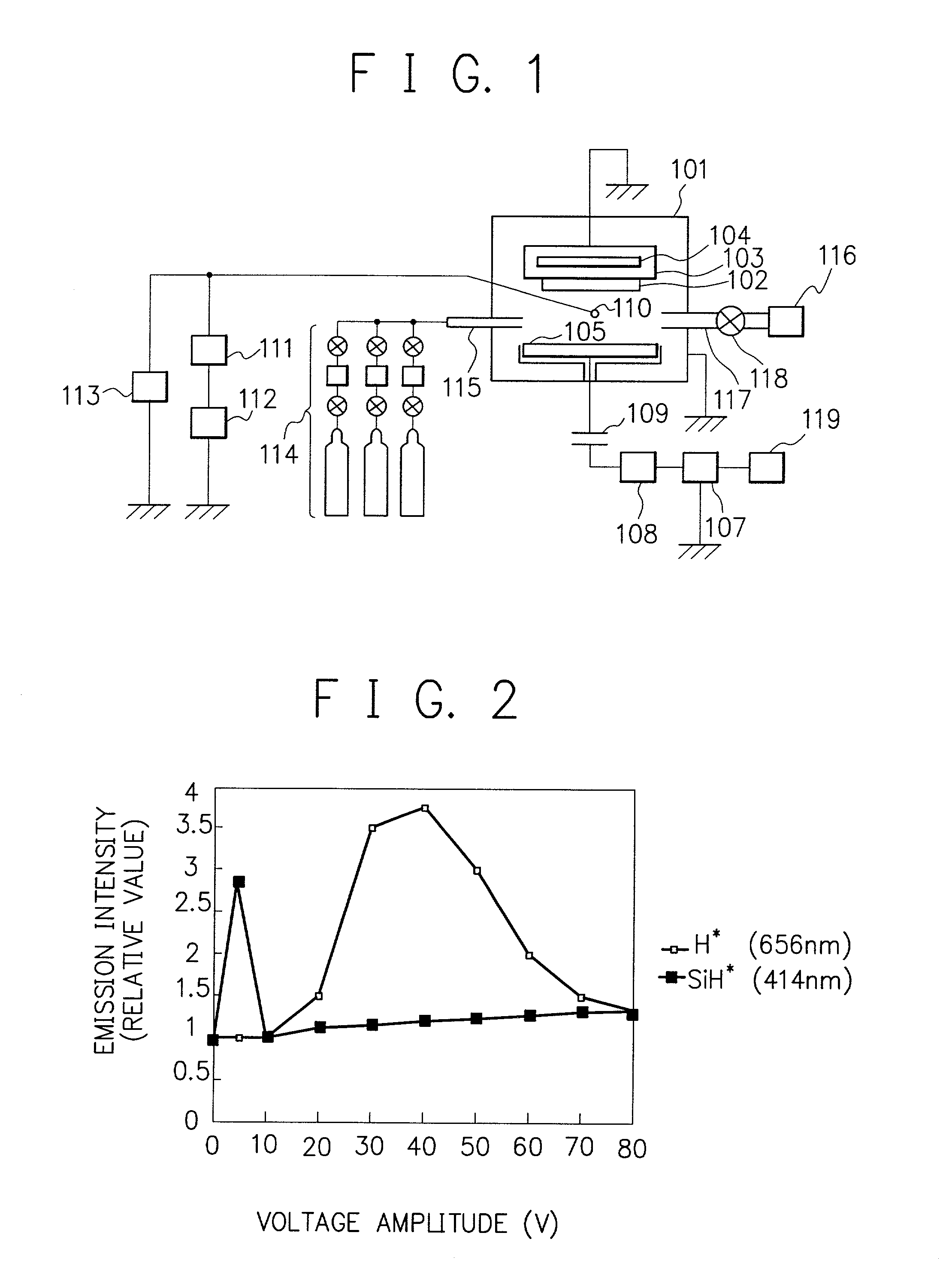
[0122] In this example, the formation of a non-single crystal silicon deposited film was conducted using the film-forming apparatus shown in FIG. 1, where a periodicity voltage of providing a negative maximum value with respect to a potential difference to the potential of the plasma generated in the film-forming vessel 101 was applied to the auxiliary electrode 110 comprising a cylindrical electrode made of a stainless steel having a diameter of 5 mm and a length of 35 cm. And observation was conducted of the generation quantity of hydrogen radical (H*) and that of SiH radical (SiH*) in the vicinity of the substrate 102 with respect to maximum amplitudes of the voltage.

[0123] Separately, for the comparison purpose, the formation of a non-single crystal silicon deposited film was conducted using a conventional plasma CVD film-forming apparatus not having such auxiliary electrode as in the present invention, and observation was conducted of the generation quantity of hydrogen radical...

example a2

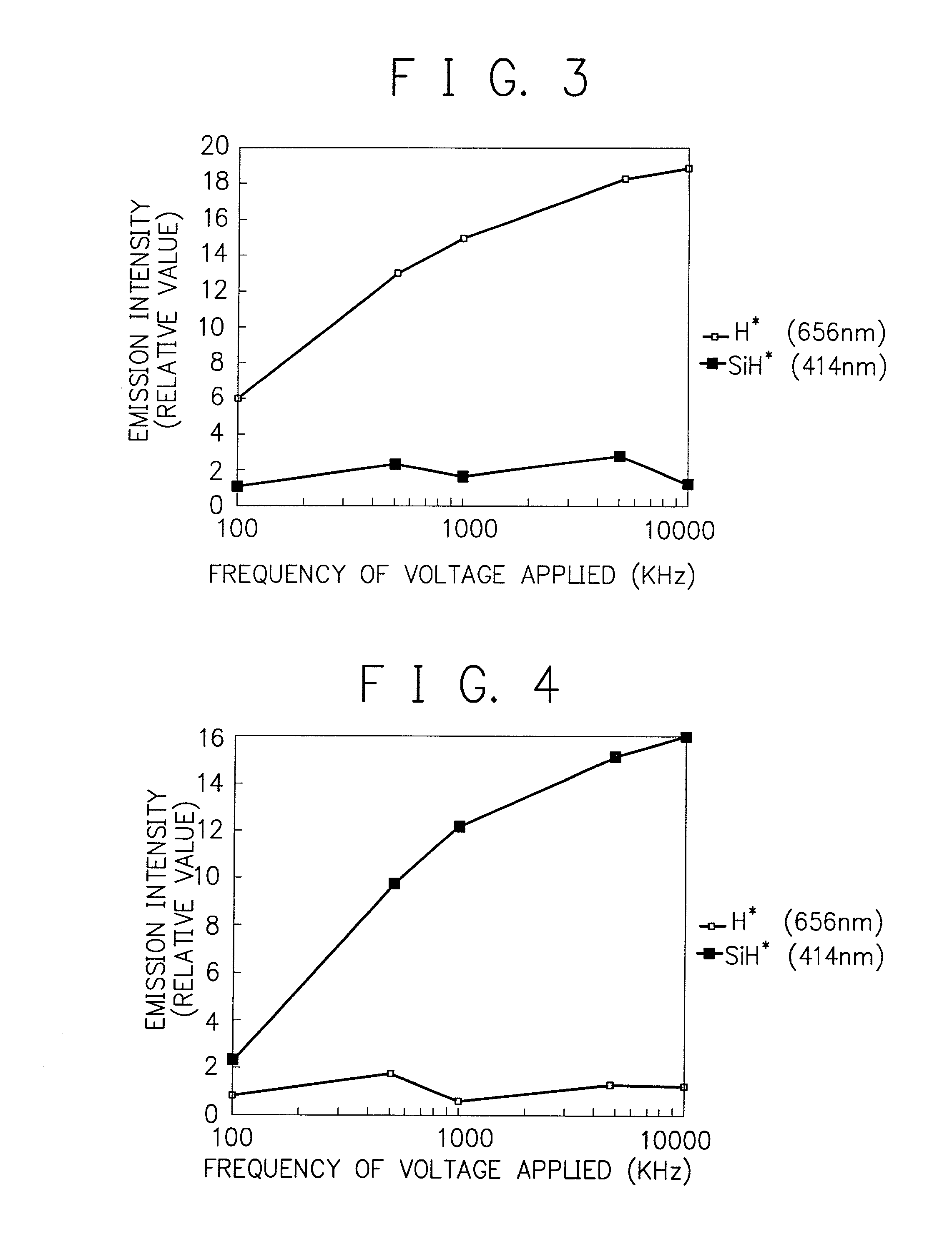
[0142] In this example, examination was conducted of the case where the frequency of the high frequency power applied to the discharge electrode 105 was made to be 60 MHz. Particularly, the film-forming procedures of Example A1 were repeated except that the frequency of the high frequency power applied to the discharge electrode 105 was changed to 60 MHz, the flow rate of the H.sub.2 gas was changed to 600 ml / minute (normal), and the inner pressure of the film-forming vessel upon the film formation was changed to 133 Pa. The film-forming procedures are repeated four times. In each case, one of the periodicity voltage of the waveform A, the periodicity voltage of the waveform B, the periodicity voltage of the waveform C, and the periodicity voltage of the waveform D was applied to the auxiliary electrode 110 in order to examine the possibility of individually controlling the quantity of SiH* and that of H* generated in the vicinity of the substrate, as well as in Example A1.

[0143] Th...


PUM

PropertyMeasurementUnit
frequencyaaaaaaaaaa
frequencyaaaaaaaaaa
frequencyaaaaaaaaaa

Abstract

A film-forming method for forming a deposited film on a substrate arranged in a substantially enclosed film-forming vessel by means of plasma CVD by introducing a raw material gas comprising at least a hydrogen gas and a silicon-containing raw material gas into said film-forming vessel and introducing a high frequency power into said film-forming vessel through a discharge electrode provided in said film-forming vessel to generate a plasma in a plasma generation region between said substrate and said discharge electrode in said film-forming vessel whereby forming said deposited film on said substrate, wherein the formation of said deposited film on said substrate is performed while applying a periodicity voltage having at least two different waveform components having a different amplitude to an auxiliary electrode arranged at a position in said plasma generation region of said film-forming vessel or an auxiliary electrode provided on the rear side of said substrate and outside said plasma generation region.

Description

[0001] 1. Field of the Invention[0002] The present invention relates to a method for forming a functional deposited film on a substrate by means of plasma chemical vapor deposition (hereinafter referred to simply as "plasma CVD"). More particularly, the present invention relates to a film-forming method by means of plasma CVD which enables one to efficiently form a high quality non-single crystal silicon series functional deposited film (such as a high quality amorphous silicon series functional deposited film or a high quality microcrystalline silicon series functional deposited film) having a homogeneous property over the entirety of a desired substrate having a large area at a high deposition rate, said deposited film being usable as a semiconductor element for semiconductor devices such as photovoltaic devices including solar cells, electrophotographic photosensitive devices (or electrophotographic light receiving members), image input line sensors, image pickup devices, and thi...

Claims


Application Information

Patent Timeline
Patent Type & Authority Applications(United States)
IPC IPC(8): C23C16/509H01L31/18H01L31/20
CPCC23C16/509H01J37/32009H01L31/1824H01L31/202Y02E10/545
Inventor KOIKE, ATSUSHIKANAI, MASAHIRO
Owner CANON KK
Why Eureka
Try Eureka