

Apparatus for decelerating ion beams for reducing the energy contamination
a technology of ion beams and ion beams, which is applied in electrical apparatus, electrical discharge tubes, nuclear engineering, etc., can solve the problems of energy contamination, difficulty in focusing beam optics, and deeper dopant depth profiles, etc., to achieve accurate control of the energy range of charged ions, accurate control of the implanting energy of charged ions, and low energy implant
- Summary
- Abstract
- Description
- Claims
- Application Information
AI Technical Summary
Benefits of technology
Problems solved by technology
Method used
Image

Examples
Embodiment Construction
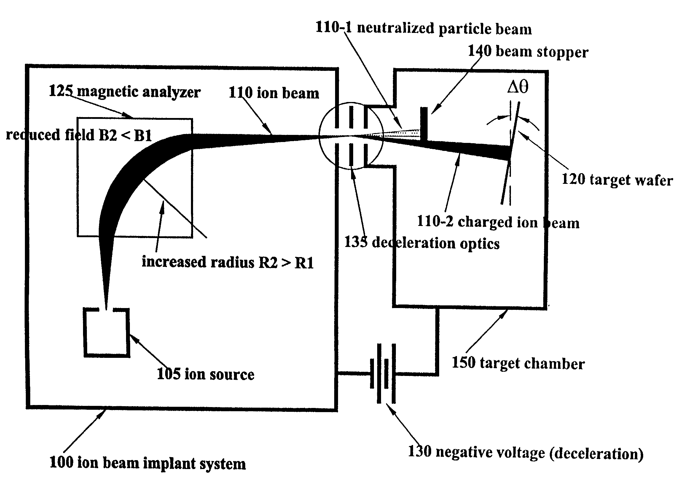
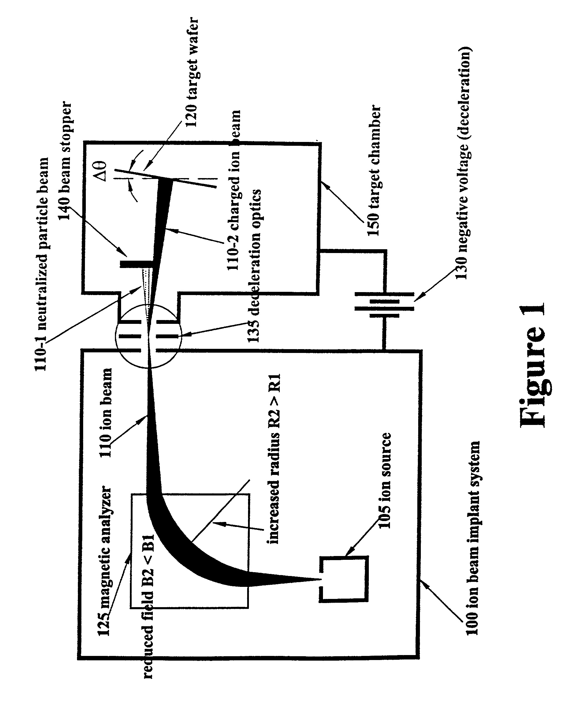
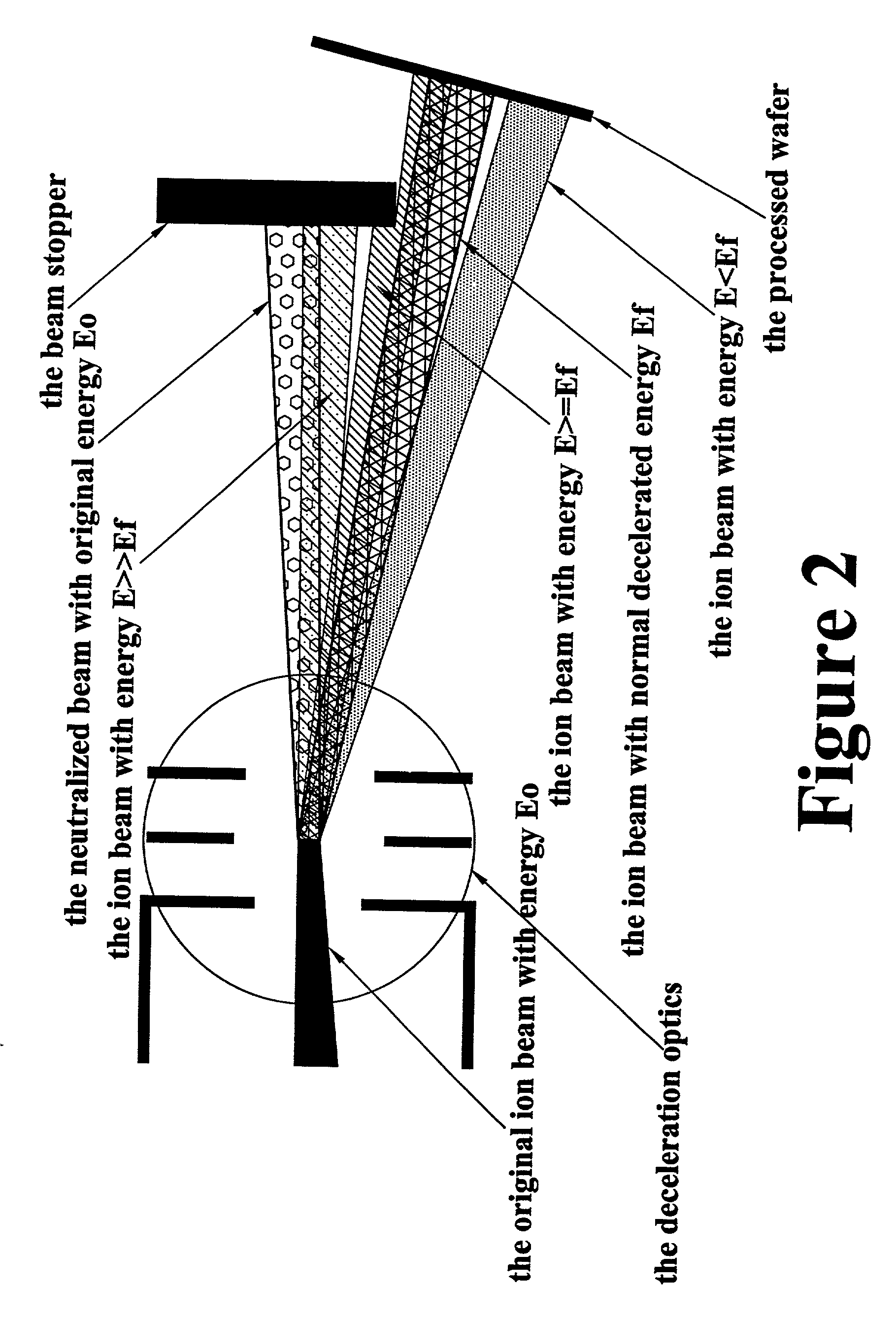
[0004] Technical difficulties of energy contamination is still a challenge faced by a person of ordinary skill in the art of semiconductor industry, particular for ion implantation with implanting energy less than one KeV. Specifically, as the dimension of the semiconductor device continues to shrink in the last decade, for the device with dimension of 0.18 .mu.m or less, ion energies for ion implantation should be 1 keV or less to form shallow junctions. This is particularly true for implantation of boron ions. For a conventional high current ion implanter, an ion beam is extracted from an ion source, travels through a mass analyzer, and then reaches semiconductor wafers. The travel distance from the source to the wafers is usually about two meters. For an ion beam with energy as low as 0.2 keV and beam current as high as 10 mA, the space charge of the beam is so high that the ion beam starts to blow up severely as soon as it gets out of the source. This difficulty exists regardles...
PUM
 Abstract
Description
Claims
Application Information