Interferometer and its fabrication method

Inactive Publication Date: 2002-09-12
NIPPON TELEGRAPH & TELEPHONE CORP
View PDF9 Cites 34 Cited by
  • Summary
  • Abstract
  • Description
  • Claims
  • Application Information

AI Technical Summary

Benefits of technology

0030] In particular, using the thin film heaters in the local annealing obviates the need for high accuracy alignment of the irradiation position at the local annealing. Thus, simply supplying current to a predetermined thin film heater is enough to achieve the trimming, thereby enabling the trimming using a rather simple device, which is very advantageous in putting the device in accordance with the present invention into practical

Problems solved by technology

The high temperature process causes thermal stress in the glass film constituting the waveguides, resulting in waveguide birefringence (B-value) in which the effective refractive index of the waveguide varies depending on the polarization state, thereby bringing about optical polarization dependency in the circuit characteristics.
In addition, since the waveguide birefringence differs slightly in a wafer surface because of fabrication error, it is necessary to trim the waveguide birefringence locally for each optical circuit to achieve satisfactory optical circuit characteris

Method used


Image

  • Interferometer and its fabrication method
  • Interferometer and its fabrication method
  • Interferometer and its fabrication method

Examples


Example

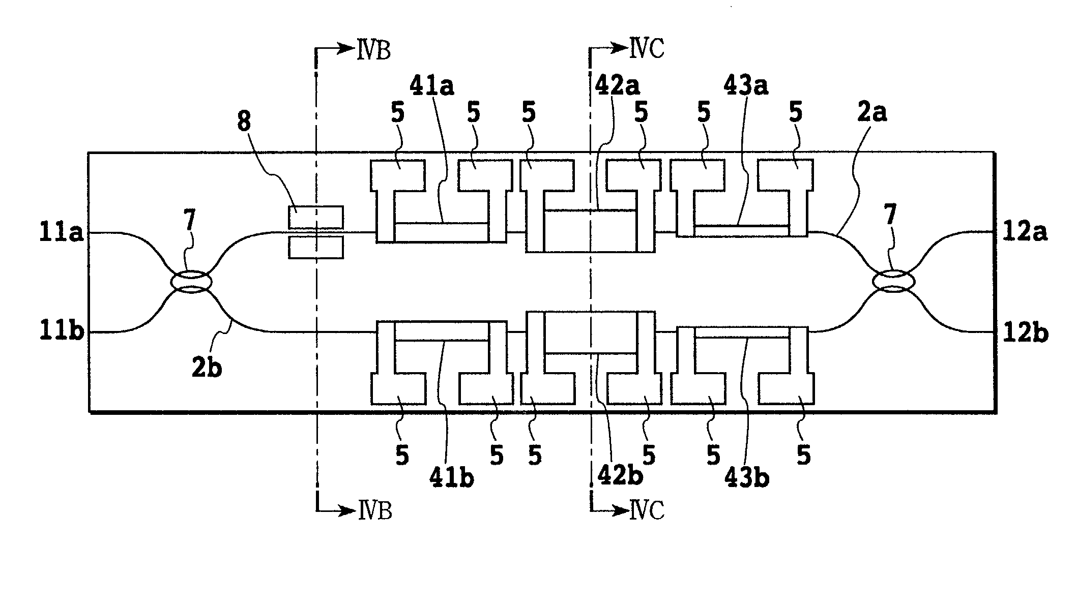
[0076] FIGS. 4A-4C shows a configuration of a polarization beam splitter (PBS) of a first embodiment used as an interferometer. Here, FIG. 4A is a plane view, FIG. 4B is a cross-sectional view taken along the line IVB-IVB of FIG. 4A, and FIG. 4C is a cross-sectional view taken along the line IVC-IVC of FIG. 4A. In FIGS. 4A-4C, the reference numeral 8 designates a stress releasing groove (.lambda. / 2 polarization dependent delay means), reference numerals 41a and 41b each designate a local annealing thin film heater (ww.sub.o), 42a and 42b each designate a local annealing thin film heater (w >w.sub.o), and 43a and 43b each designate a local annealing thin film heater (w

[0077] The PBS comprises, on an MZI that is composed of two 50% (3dB) optical couplers 7 and 7, two waveguide arms 2a and 2b linking the two couplers, and input / output waveguides connecting input / output ports with the couplers, the .lambda. / 2 polarization dependent delay means 8 for providing the MZI with the...

Example

[0100] FIGS. 6A-6C show a configuration of a polarization beam splitter (PBS) in a second embodiment used as an interferometer. FIG. 6A is a plane view, FIG. 6B is a cross-sectional view taken along the line VIB-VIB of FIG. 6A, and FIG. 6C is a cross-sectional view taken along the line VIC-VIC of FIG. 6A. Although the configuration is similar to that of the PBS of the first embodiment, it differs in that the number and types of the thin film heaters are reduced. Specifically, it comprises only two types of thin film heaters, a 15 .mu.m (w.sub.o) wide thin film heater 42, each assigned to one of the arms as a local annealing(heating) means. In addition, the stress releasing grooves 8 as a .lambda. / 2 polarization dependent delay means are designed slightly shorter at 1.7 mm so that the polarization dependency difference .DELTA.L.sub.p of the optical path length difference between the waveguide arms becomes always less than .lambda. / 2 (that is, L.sub.p(o)<.DELTA.L.sub.p(f)).

[0101] The ...

Example

[EMBODIMENT 3: PBS3]

[0106] FIGS. 7A and 7B shows a configuration of a polarization beam splitter (PBS) used as an interferometer of a third embodiment. FIG. 7A is a plane view; and FIG. 7B is a cross-sectional view taken along the line VIIB-VIIB of FIG. 7A. The configuration is similar to the PBS of the second embodiment except that it does not comprise the .lambda. / 2 polarization dependent delay means, but comprises a plurality of thin film heaters 43a-43d with the same structure and thin film heaters 42a-42d with the same structure as the local annealing(heating) means. In addition, the PBS has the optical path length difference of .lambda. / 2 with making the upper waveguide slightly longer in order to level out the amounts of the heating power as will be described later. The total length of the thin film heaters, that is, the total length of the local annealing regions, is increased from that of the second embodiment by 20 mm considering the trimming amount in this embodiment.

[010...


PUM


Abstract

An interferometer includes a waveguide core, and thin film heaters with widths W1 and W2. The thin film heaters are mounted directly above the waveguide core, and operate as two types of different annealing regions. The annealing, which is carried out by supplying current to the thin film heaters, can alter the quality of the cladding, and change the stress applied on the waveguide core, thereby making it possible to control the polarization dependency. Thus changing the width of the thin film heaters and/or the amount of the supply current thereto enables the permanent control of the effective refractive index (birefringence index) independently in the transverse electric polarization mode and the transverse magnetic polarization mode. This enables the transverse electric polarization mode to be adjusted to a phase difference of .lambda./2, and the transverse magnetic polarization mode to a phase difference of zero.

Description

[0001] This application is based on Patent Application No. 2001-017943 filed Jan. 26, 2001 in Japan, the content of which is incorporated hereinto by reference.BACKGROUND OF THE INVENTION[0002] 1. Field of the Invention[0003] The present invention relates to an interferometer and its fabrication method, which enable planar optical waveguide circuits used in optical communication field to adjust optical path lengths (phases) independently in the transverse electric (TE)polarization mode and transverse magnetic (TM) polarization mode.[0004] 2. Description of the Related Art[0005] Optical circuits employing single mode waveguides formed on a substrate are characterized by high integration and mass productivity, and hence they are essential to construct economical optical network nodes. In particular, optical circuits utilizing silica-based waveguides with SiO.sub.2 as the main ingredient has favorable characteristics such as low loss, superiority in an affinity for silica-based optical...

Claims


Application Information

Patent Timeline
IPC IPC(8): G02B6/126G01B9/02G02B6/12G02B6/13
CPCG02B6/12007G02B2006/12166G02F1/2255
Inventor GOH, TAKASHIABE, MAKOTOINOUE, YASUYUKIOKUNO, MASAYUKISAIDA, TAKASHI
Owner NIPPON TELEGRAPH & TELEPHONE CORP
Why Eureka
Try Eureka