Time-multiplexing data between asynchronous clock domains within cycle simulation and emulation environments

Inactive Publication Date: 2002-09-12
GLOBALFOUNDRIES INC
View PDF10 Cites 27 Cited by
  • Summary
  • Abstract
  • Description
  • Claims
  • Application Information

AI Technical Summary

Benefits of technology

0015] The invention addresses these and other problems associated with the prior art by providing an apparatus and method that utilize a buffer interposed in a common signal path between asynchronous clock domains in a hardware-based emulation environment to manage the communication of time-multiplexed data signals bet

Problems solved by technology

With increases in circuit complexity, however, the processes of designing and testing circuit designs become increasingly complex and time consuming.
However, with the increasingly complex nature of many circuit designs, software-based simulation is often too time consuming and inefficient.
While the use of the aforementioned connectors between processor chips often provides adequate connectivity between processors, the interconnection mechanism is typically not capable of supporting asynchronous communications between processors with the same degree of connection density.
While many logic emulators support the ability to emulate multiple clock domains, communicating signals between clock domains is problematic, since the receiver of an asynchronous signal has no clock relationship to the source, and

Method used


Image

  • Time-multiplexing data between asynchronous clock domains within cycle simulation and emulation environments
  • Time-multiplexing data between asynchronous clock domains within cycle simulation and emulation environments
  • Time-multiplexing data between asynchronous clock domains within cycle simulation and emulation environments

Examples


Embodiment Construction

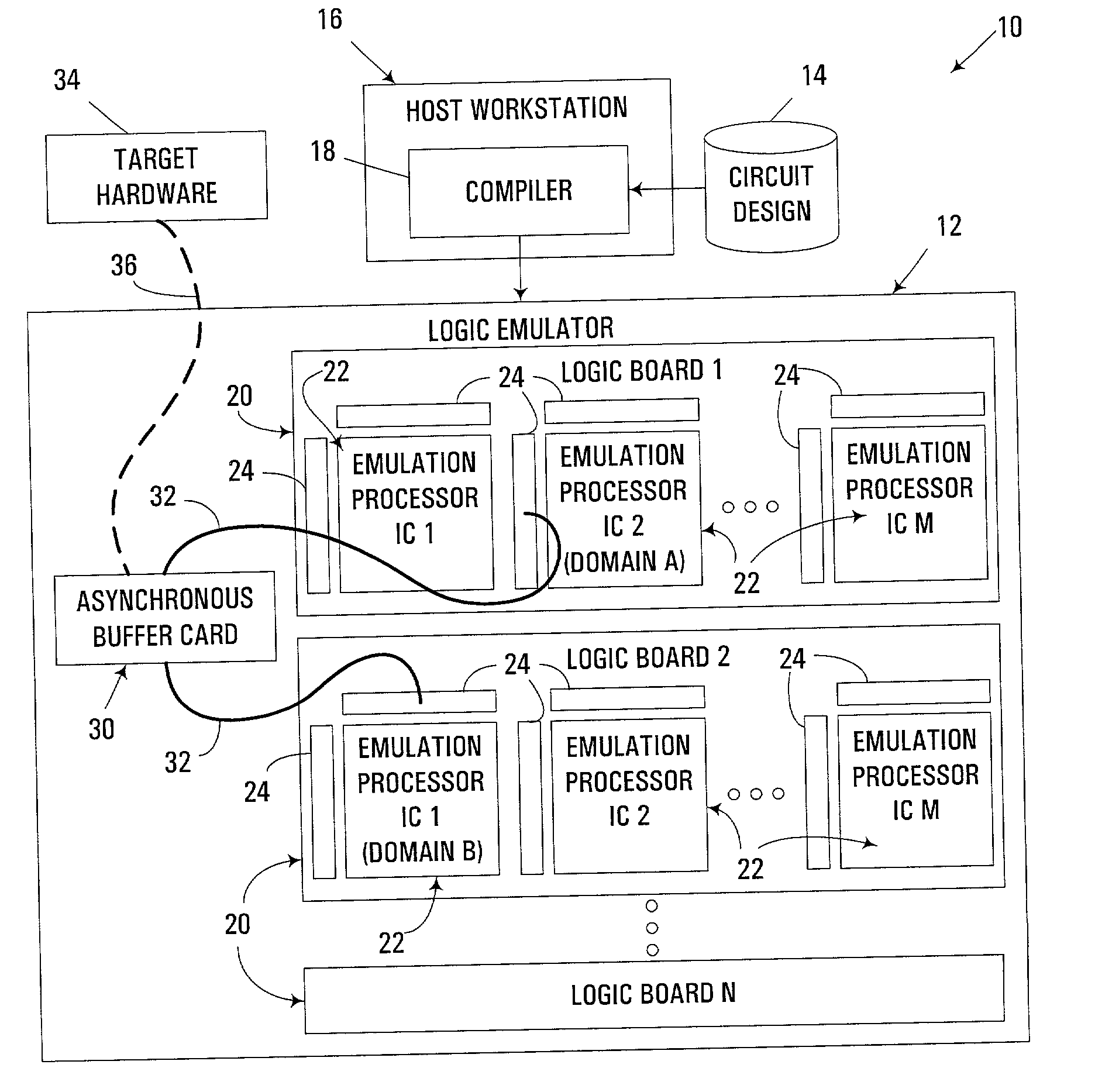
[0022] Turning to the Drawings, wherein like numbers denote like parts throughout the several views, FIG. 1 illustrates a hardware-based logic emulation system 10 consistent with the invention. System 10 includes a hardware-based logic emulator 12, which is used to emulate a circuit design stored in a database 14. The circuit design is typically designed and modeled in a high-level hardware definition language such as Verilog or VHDL. The logic emulator 12 operates on a gate-level compiled model of the circuit design, which may be generated, for example, on a host workstation 16 that executes a compiler 18. The host workstation may also be used to design or perform other Electronic Design Automation (EDA) steps during the development, testing, verification and / or validation of a circuit design.

[0023] Logic emulator 12 may be based upon any number of suitable hardware-based logic emulation or simulation environments, e.g., the ET3.5 emulation environment from International Business M...


PUM


Abstract

An apparatus and method utilize a buffer interposed in a common signal path between asynchronous clock domains in a hardware-based logic emulation environment to manage the communication of time-multiplexed data signals between the clock domains during hardware-based emulation. The buffer is effectively used to latch each data signal communicated across the common signal path so that the clock domain that receives the signals can retrieve each such signal at appropriate points in the receiver clock domain's evaluation cycle. Independently-controlled write/read pointers are maintained in a buffer control circuit to independently address the buffer for the transmitter and receiver sides of an asynchronous communication path. Locations in the buffer are associated with specific steps in the evaluation cycles of each of the transmitter and receiver clock domains, and the write/read pointers are managed to respectively write and read data to and from the locations in the buffer based upon the current evaluation steps being performed within the respective evaluation cycles of the transmitter and receiver clock domains.

Description

FIELD OF THE INVENTION[0001] The invention is generally related to simulation and emulation of integrated and other electronic circuit designs. More specifically, the invention is generally related to the communication of data within a hardware-based cycle simulation or emulation environment.BACKGROUND OF THE INVENTION[0002] As semiconductor fabrication technology advances, designers of integrated circuits and electronic circuits incorporating the same are able to integrate more and more functions into individual integrated circuit devices, or chips. As such, electronic designs that once required several integrated circuits electrically coupled to one another on a circuit board or module may now be integrated into fewer integrated circuits, thereby increasing performance and reducing cost.[0003] With increases in circuit complexity, however, the processes of designing and testing circuit designs become increasingly complex and time consuming. As a result, computers have become incre...

Claims


Application Information

Patent Timeline
IPC IPC(8): G01R31/28G06F9/455G06F17/50H03K19/00
CPCG06F17/5022G06F30/33
Inventor GOODING, THOMAS MICHAELMUSSELMAN, ROY GLENNNEWSHUTZ, ROBERT N.RUEDINGER, JEFFREY JOSEPH
Owner GLOBALFOUNDRIES INC
Why Eureka
Try Eureka