

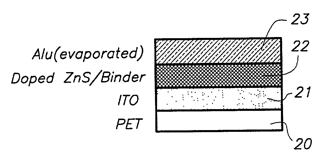
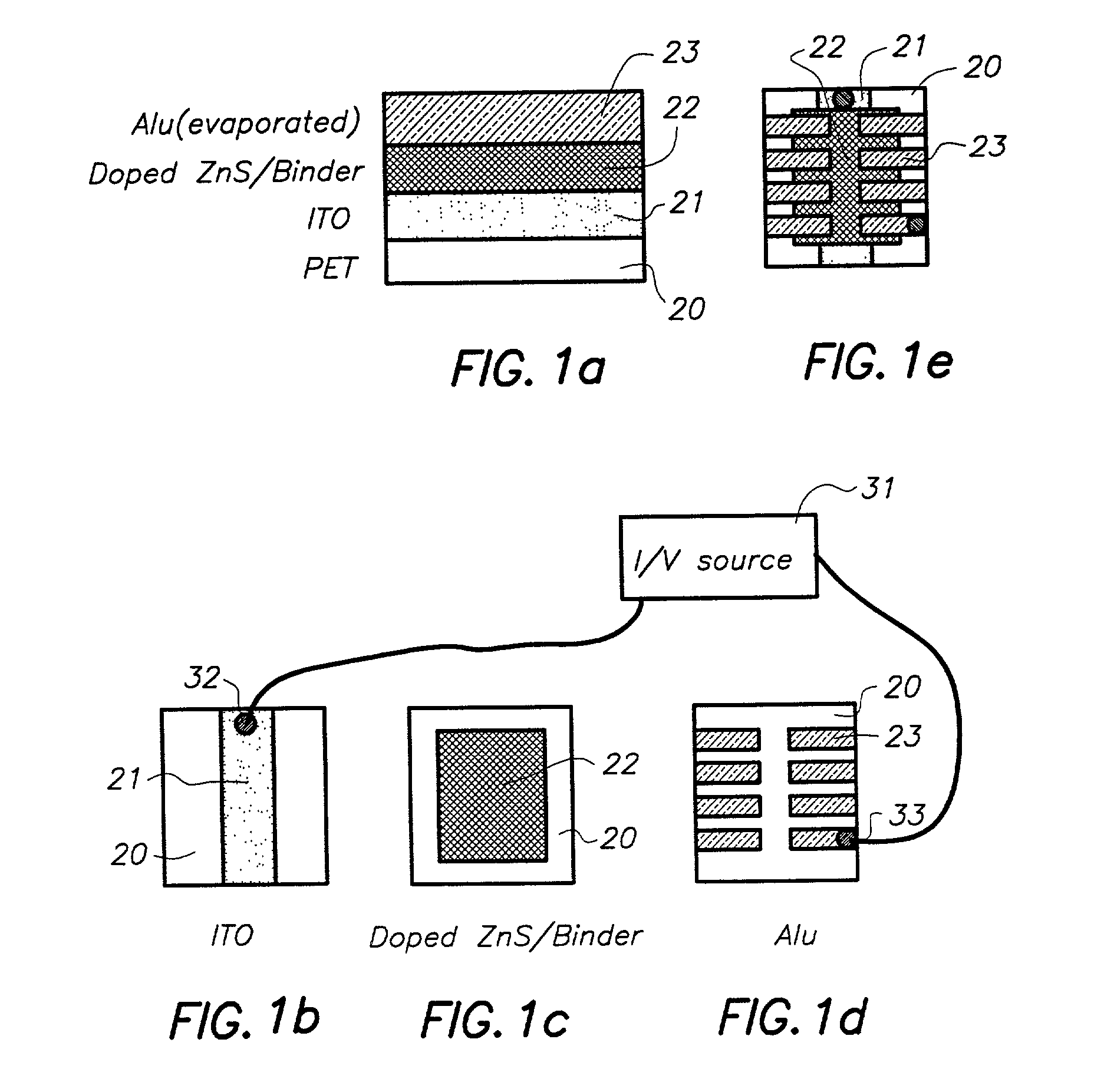
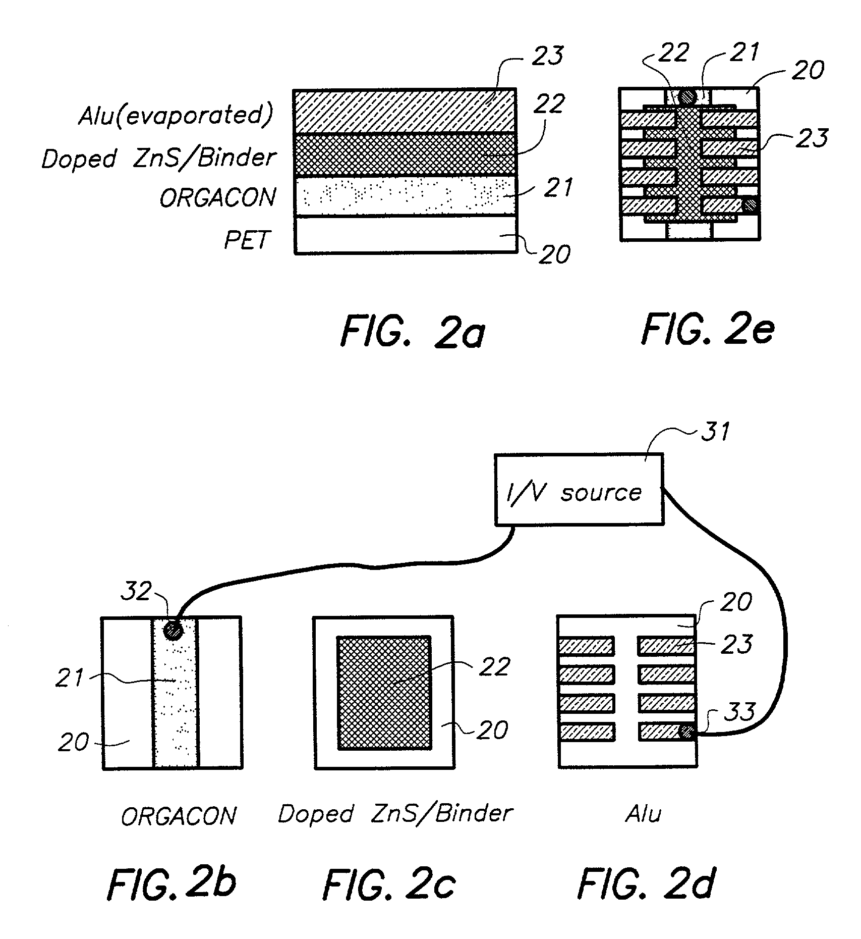
Manufacturing of a thin film inorganic light emitting diode
a technology of inorganic light and diodes, which is applied in the manufacture of electric discharge tubes/lamps, hose connections, and discharge tubes luminescnet screens, etc., can solve the problems of low fluorescent quantum yield, cumbersome and expensive vacuum-vapour deposition techniques, and low fluorescent quantum yield of tfel devices, etc., to achieve easy and economical
- Summary
- Abstract
- Description
- Claims
- Application Information
AI Technical Summary
Benefits of technology
Problems solved by technology
Method used
Image

Examples
Embodiment Construction
[0064] 1. Green emitting single layer ILEDs
[0065] 1.1. Preparation of the Zn(Cu(0.05%))S-dispersion:
[0066] The following solutions were,prepared:
1 Solution 1 Zn(acetate).sub.2.2H.sub.2O 131.7 g Na.sub.4EDTA 12 g Cu(acetate).sub.2.4H.sub.2O 54 mg Water to 600 ml Solution 2 Na.sub.2S.9H.sub.2O 113.6 g NH.sub.3 (26%) 5 ml Water to 600 ml Solution 3 5-methyl-1,2,4-triazolo-(1,5-a)-pyrimidine-7-ol 40 g NaCl 58.44 g Water to 600 ml
[0067] The ZnS:Cu(0.05%) dispersion was prepared as follows:
[0068] To solution 3, stirred at 1500 rpm at room temperature solutions 1 and 2, both held at room temperature, were added simultaneously at a flow rate of 500 ml / min. This is the predispersion A comprising ZnS:Cu--particles.
[0069] 1.2. Washing of the ZnS:Cu--dispersion:
[0070] To 1000 ml of predispersion A, 1000 ml of a 2% polyphosphoric acid solution in water was added and this dispersion was diafiltrated through a Fresenius F60 cartridge. The dispersion was concentrated to 1000 ml and washed at this l...
PUM
 Abstract
Description
Claims
Application Information