CMOS structure with maximized polysilicon gate activation and a method for selectively maximizing doping activation in gate, extension, and source/drain regions

a polysilicon gate and polysilicon gate technology, applied in the field of semiconductor devices, can solve the problems of insufficient activation, insufficient impurity concentration, and excessive lateral diffusion of dopants

Inactive Publication Date: 2002-11-21
GLOBALFOUNDRIES US INC
View PDF0 Cites 18 Cited by
  • Summary
  • Abstract
  • Description
  • Claims
  • Application Information

AI Technical Summary

Benefits of technology

[0012] An advantage of the present invention is to achieve maximized polysilicon gate activation while preventing source / drain regions from being doped at an excessively high impurity concentration, and thereby avoiding lateral encroachment of the dopant into the channel. Another advantage of the present invention is to provide a production-worthy manufacturing method for maximization of gate electrode activation without significant modification of the processing steps and equipments. A further advantage of the present invention is to provide a precisely calibrated annealing step with an optimal temperature and thermal cycle depending on the dopant type implanted in the gate electrode. Furthermore, the present invention provides various manufacturing sequences to achieve the maximum gate electrode activation.
[0013] Additional advantages and other features of the present invention will be set forth in part in the description which follows and will become apparent to those having ordinary skill in the art upon examination of the following or may be learned from the practice of the present invention. The objects and advantages of the present invention may be realized and obtained as particularly pointed out in the appended claims.
[0014] According to the present invention, the foregoing and other advantages are achieved in part by a method for manufacturing a semiconductor device, comprising the step of forming source / drain regions of a first conductivity type in a main surface of a semiconductor substrate, and selectively doping a gate electrode formed on said main surface, so that said gate electrode has an impurity concentration of said first conductivity type higher than that of said source / drain regions.
[0015] According to certain embodiments of the present invention, the gate electrode is fully doped by two steps. First, the gate electrode is partially doped by a separate ion implantation step while the source / drain regions are masked. Then, the gate electrode is fully doped when the source / drain regions are formed by ion implantation.
[0016] Thus, according to the present invention, the gate electrode is doped at an optimized impurity implantation concentration, independently from the impurity implantation for the source / drain regions. Accordingly, the present invention enables maximization of the gate electrode activation while preventing the source / drain regions from being doped at an excessively high impurity concentration.

Problems solved by technology

Therefore, for devices having a gate length smaller than 0.1 .mu.m, excessively high concentration doping for the source and drain regions causes excessive lateral diffusion of the dopants (e.g., boron, phosphorous) into the channel region.
This causes insufficient impurity concentration for the polysilicon gate, insufficient activation of a polysilicon gate, and eventually a gate depletion problem when a bias current is applied to the gate to turn on the MOSFET device.
This in turn results degradation of the device performance, such as reduction of the output current due to the increased effective gate dielectric thickness.
However, such a short thermal cycle during the annealing step is not sufficient to fully activate the implanted dopants in the polysilicon gate.
Thus, if an annealing step is performed to activate source / drain regions only, the gate electrode may not be fully activated.
As a possible alternative, a metal gate has been introduced, but it has been found that it is difficult and costly to achieve a proper work function difference between an N-type MOS transistor and a P-type MOS transistor.
Therefore, a metal gate is not considered to be a suitable or successful solution to obtain optimal transistor performance consistent with manufacturing economy.

Method used


Image

  • CMOS structure with maximized polysilicon gate activation and a method for selectively maximizing doping activation in gate, extension, and source/drain regions
  • CMOS structure with maximized polysilicon gate activation and a method for selectively maximizing doping activation in gate, extension, and source/drain regions
  • CMOS structure with maximized polysilicon gate activation and a method for selectively maximizing doping activation in gate, extension, and source/drain regions

Examples


first embodiment

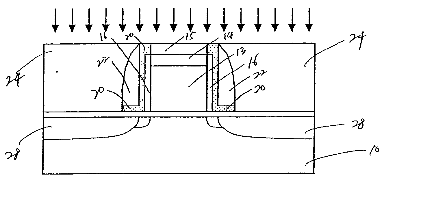
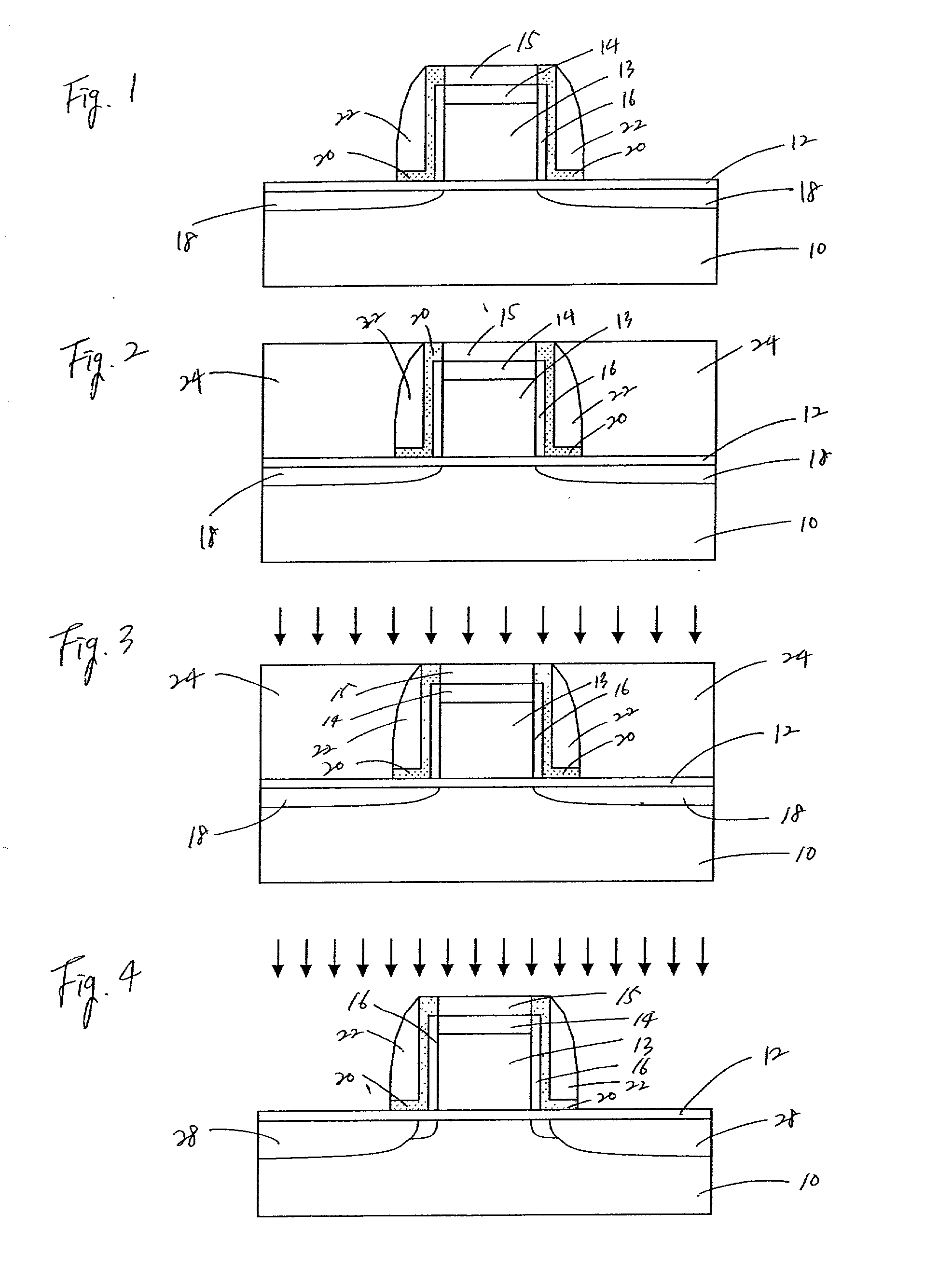
[0023] With this in mind, referring now to the drawings, FIGS. 1-4 depict a method for manufacturing such device according to the present invention. In FIG. 1, there is shown a sectional view of a semiconductor device, in which a gate electrode 13 is formed on a semiconductor substrate 10 with a gate oxide layer 12 therebetween. On the upper surface of the gate electrode 13, an oxide cap layer 14, a nitride cap layer 15 are formed. On the side surfaces of the gate electrode 13, oxide sidewalls 17, a nitride liner 20 and sidewall spacers 22 are formed.

[0024] As conventionally well known, this gate structure can be formed by sequentially depositing a polysilicon layer, an oxide layer (e.g., TEOS) and a nitride layer on the gate oxide layer 12. The layers are etched by conventional lithographic and etching techniques (e.g., reactive ion etching) to shape the gate electrode 13. Preferably, these layers are patterned to form the gate electrode 13 having a gate length smaller than about 0...

second embodiment

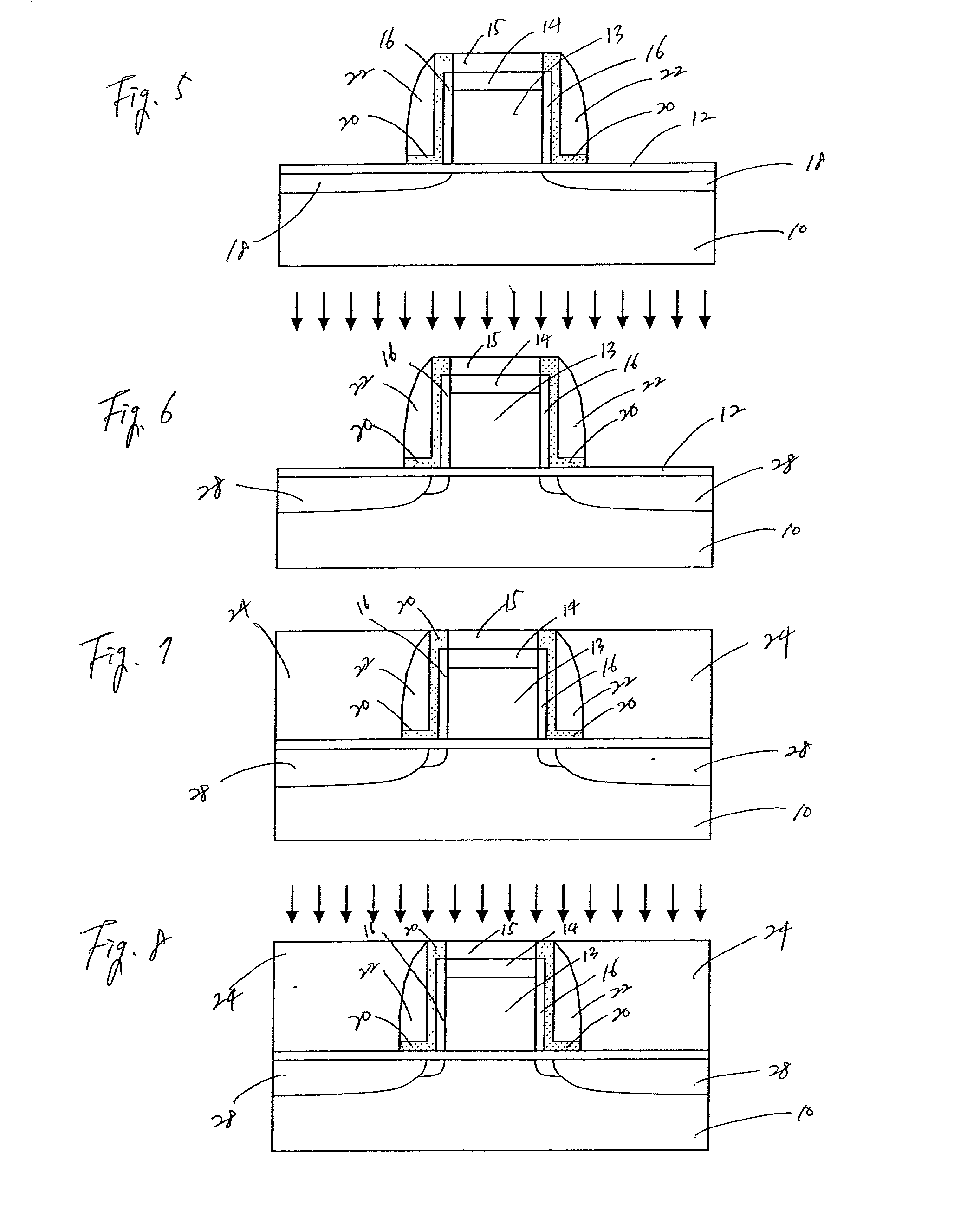
[0037] FIGS. 5 to 8 depict manufacturing steps according to the present invention. The method according to this embodiment involves a slightly different process sequence from the previous embodiment. Thus, the present invention can be implemented in various ways, as readily conceivable from the exemplary embodiments shown herein, and is not limited to certain processing sequences shown herein.

[0038] According to the second embodiment, gate doping is performed by two steps. First, the gate electrode is doped during the source / drain implantation step at the impurity concentration predetermined for the source / drain formation and activation, which is not sufficient for the maximum gate activation. To compensate the deficiency in the impurity concentration for the maximum activation, the gate electrode is further selectively doped to increase the chemical impurity concentration while the source / drain regions are blocked from the further impurity implantation.

[0039] With this in mind, FIG...


PUM


Abstract

A method is provided for maximizing activation of a gate electrode while preventing source and drain regions from being excessively doped. The gate electrode is partially doped when exposed the source / drain implantation step. Then, the gate electrode is fully doped by the selective implantation step while the source / drain regions are blocked. Separate annealing steps are provided subsequent to the gate doping step and the source and drain implantation step.

Description

[0001] 1. Field of the Invention[0002] The present invention generally relates to a semiconductor device, more particularly to a complementary metal oxide (CMOS) silicon field effect transistor (FET) having a polysilicon gate electrode with a sub-0.1 .mu.m gate length scale.[0003] 2. Background Description[0004] The escalating requirements for high density and performance associated with ultra large scale integration semiconductor devices involves submicron device features, high reliability and increased manufacturing throughput.[0005] Conventional practices are primarily based upon a polysilicon gate CMOS process, in which source and drain regions are formed by implanting impurity atoms in the substrate by using a polysilicon gate electrode as a mask. This has an advantage of doping the polysilicon gate simultaneously when source and drain regions are formed by ion implantation at the same implantation dose. Subsequently, annealing is performed to activate the implanted impurity at...

Claims


Application Information

Patent Timeline
Patent Type & Authority Applications(United States)
IPC IPC(8): H01L21/336H01L21/8238
CPCH01L21/823814H01L29/6659H01L21/823842
Inventor PARK, HEEMYONGSCHEPIS, DOMINIC J.ASSADERAGHI, FARIBORZ
Owner GLOBALFOUNDRIES US INC
Why Eureka
Try Eureka