
Eureka
For R&D, Eureka makes reading and utilizing patents & technical documents easy.
Eureka AIR
Designed for self-driven R&D workflows. Generate viable solutions, solve complex R&D challenges, empower your innovation with AI.

Eureka Materials
Designed for material experts only. Revolutionize your material R&D, from search, analyze, to developing new materials.

TechResearch
Generate reliable direction feasibility study reports for your R&D in just a few steps.

TechSeek
Discover and master advanced knowledge NOW. Basics, ideas, possibilities, all at once.

TechMind
As an expert in R&D Theories, TechMind can generates customized viable solutions instantly.

TechRisk
Analyze your overall solution with one click, know your potential R&D risks in advance.

TechMonitor
Get weekly tech updates, stay abreast of the latest tech innovations and key insights.
Conductive particles, conductive composition, electronic device, and electronic device manufacturing method
- Summary
- Abstract
- Description
- Claims
- Application Information
AI Technical Summary
Benefits of technology
Problems solved by technology
Method used
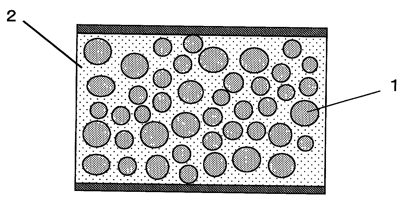
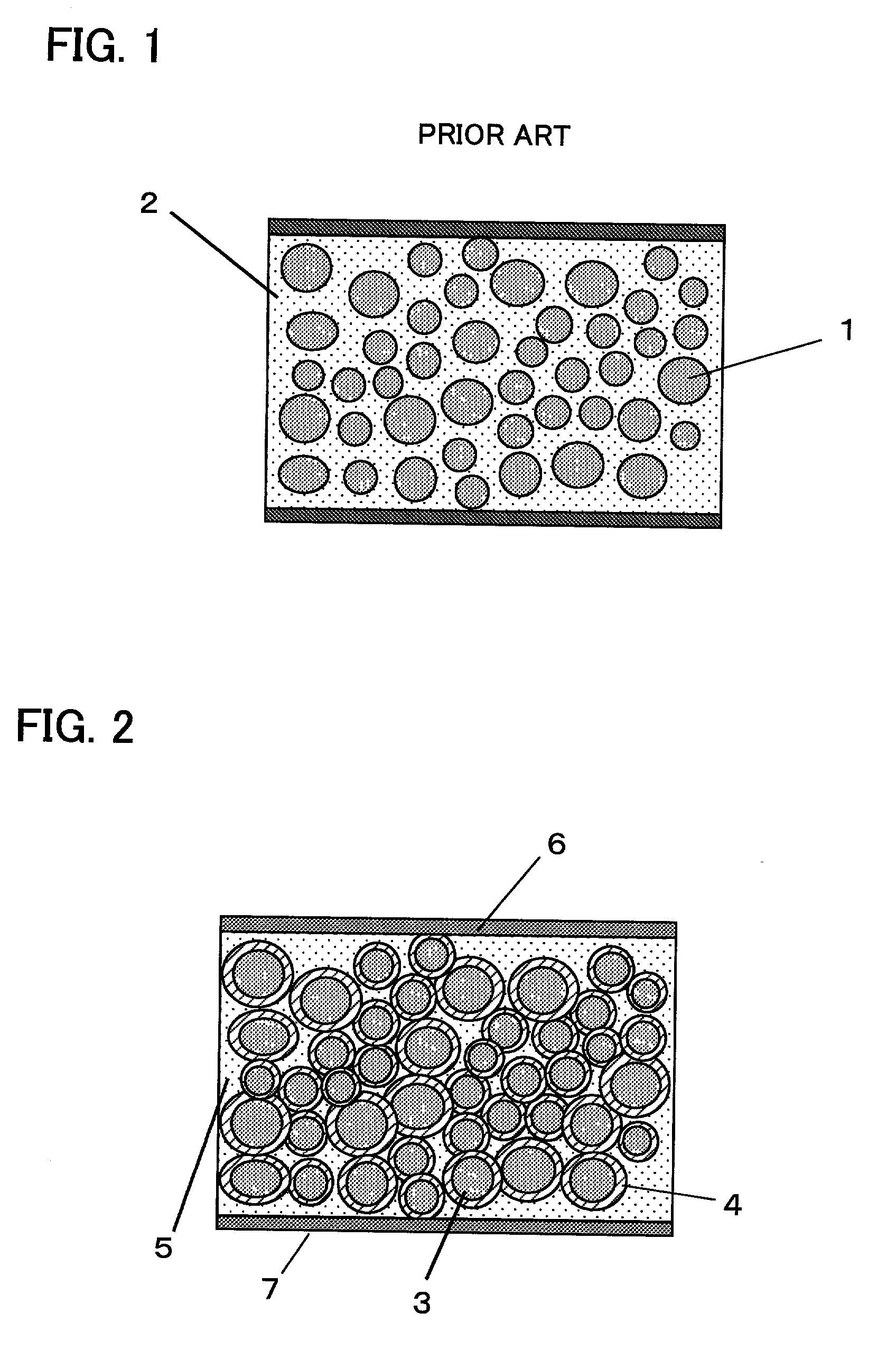
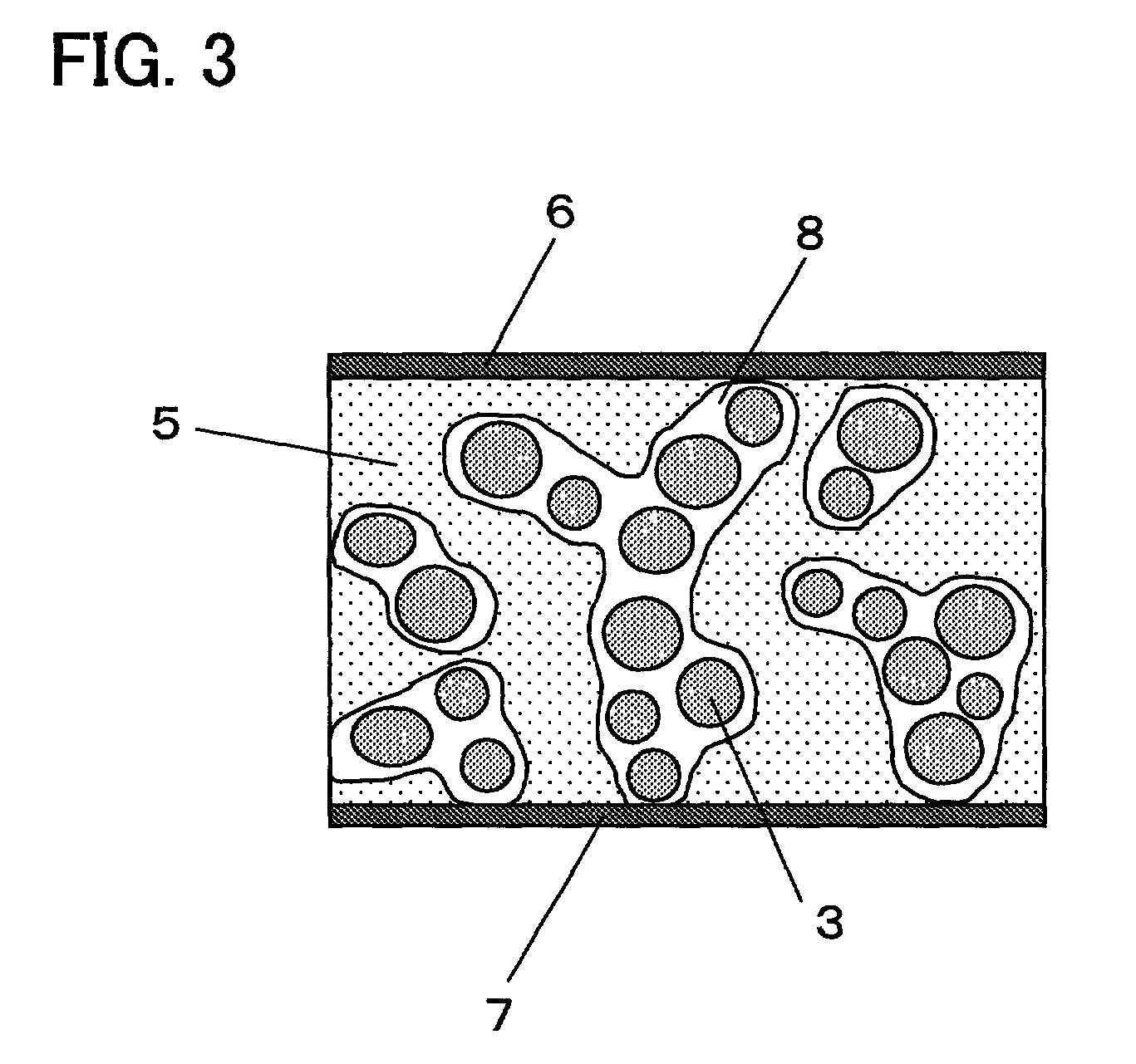
Image

Examples
example 2
[0099] On In powder base materials having an average particle size of 20 to 40 .mu.m, were formed Sn and Sn--Bi alloy to film thicknesses of approximately 2 to 4 .mu.m by electroplating, respectively, to fabricate metal fillers.
[0100] Those metal fillers (80% by weight) were then mixed and stirred together with EXA 830 LVP (20% by weight) which is a bisphenol A type epoxy resin made by Dainippon Ink and Chemicals, Inc., and the resin mixtures were cured under conditions of 150.degree. C. for 30 minutes.
[0101] The coefficients of thermal conductivity were measured by a laser flash method. The measured results are given in Table 1.
example 3
[0102] On Pb powder base materials having an average particle size of 20 to 40 .mu.m, were formed Sn--Bi alloys and Sn--In alloys to film thicknesses of approximately 2 to 4 .mu.m by electrolessplating, respectively, to fabricate metal fillers.
[0103] Those metal fillers (80% by weight) were then mixed and stirred together with EXA 830 LVP (20% by weight) which is a bisphenol A type epoxy resin made by Dainippon Ink and Chemicals, Inc., and the resin mixtures were cured under conditions of 150.degree. C. for 30 minutes.
[0104] The coefficients of thermal conductivity were measured by a laser flash method. The measured results are given in Table 1.
PUM
| Property | Measurement | Unit |
|---|---|---|
| Percent by mass | aaaaa | aaaaa |
| Percent by mass | aaaaa | aaaaa |
| Angle | aaaaa | aaaaa |
Abstract
Description
Claims
Application Information
 - R&D Engineer
- R&D Manager
- IP Professional
- Industry Leading Data Capabilities
- Powerful AI technology
- Patent DNA Extraction
Browse by: Latest US Patents, China's latest patents, Technical Efficacy Thesaurus, Application Domain, Technology Topic, Popular Technical Reports.
© 2024 PatSnap. All rights reserved.Legal|Privacy policy|Modern Slavery Act Transparency Statement|Sitemap|About US| Contact US: help@patsnap.com