Method to GaAs based lasers and a GaAs based laser

Inactive Publication Date: 2003-02-13
NORTHLIGHT AB
View PDF0 Cites 170 Cited by
  • Summary
  • Abstract
  • Description
  • Claims
  • Application Information

AI Technical Summary

Benefits of technology

0113] The new method according to the invention is based on ion-milling using nitrogen as one vital constituent. The benefits of using this method to form for example laser wave-guide structure are five-fold.
0114] The surface will be much smoother than conventional wet and dry etching methods, thereby minimizing the scattering losses.
0115] The nitrogen ion-beam milling process can form a native nitride layer, which blocks any impurity to react with the active material.
0116] The native nitride la

Problems solved by technology

Typically, the processes are complicated and involve at least two steps.
The important result was that N ions had no measurable detrimental influence on the laser diode performance while milling with Ar ions affected the performance negatively in the milling process.
The last work listed (Yu et al.) above offers another means to form a nitrided layer, but it is restricted in that an all-InN layer is not obtained.
These results show that defects that could be detrimenta

Method used


Image

  • Method to GaAs based lasers and a GaAs based laser
  • Method to GaAs based lasers and a GaAs based laser
  • Method to GaAs based lasers and a GaAs based laser

Examples


second embodiment

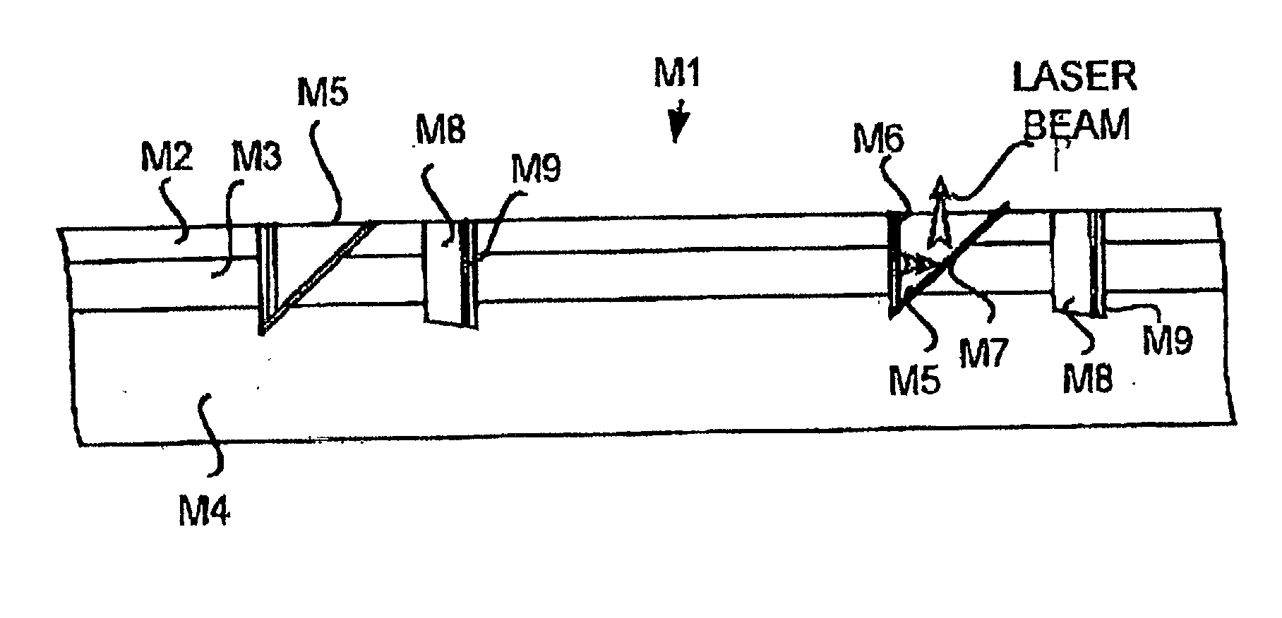
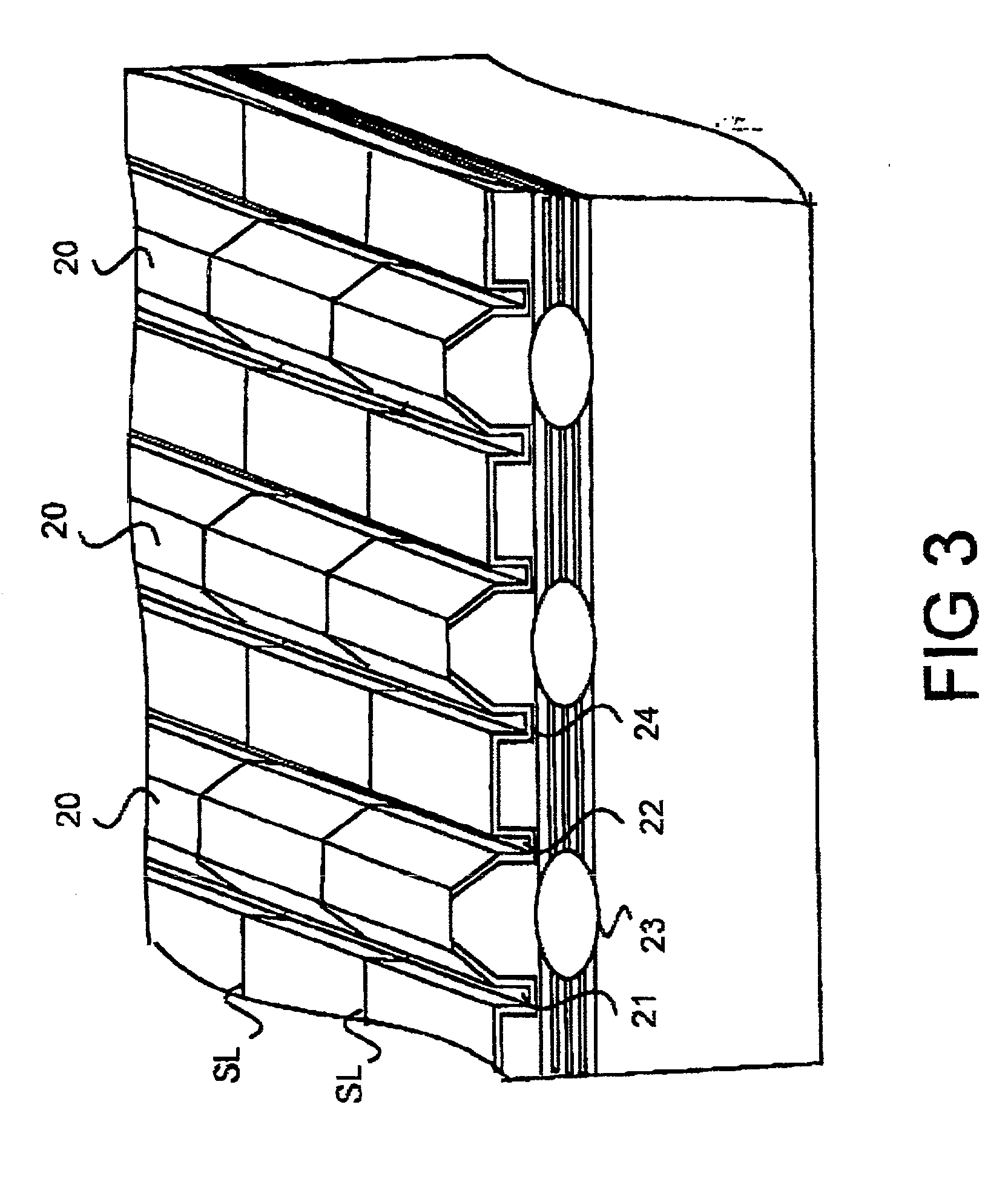
[0159] According to the invention FIG. 3 shows a wafer part with a ridge-structure 20 for each laser unit. The ridge-structure has a trench 21, 22 on each side for example to define a wave-guide 23 for the laser beam, cause current blocking, or for improved thermal conductivity. Deposition layer 24 is provided on the ridge-structure 20 and in the trenches 21, 22. In order to have the vertical sides of the trenches dry-etched and coated with the deposition layer the incident and extracted, respectively, beams are moved with alternate beam angles.

[0160] The wafer part is provided with scribe lines SL where cleaving into bars should be made. The wafer is shown without the protecting layer, which is provided onto the deposition layer in the same way as in the embodiment shown in FIG. 2.

[0161] It is the ridge, which defines the wave-guide. Current limit could be used in order to provide a single transverse mode below the ridge or mesa. Also trenches affect the mode and could give a more ...

third embodiment

[0162] Referring to FIG. 4, in which the third embodiment is shown. FIG. 4 shows a section perpendicular to those shown in FIG. 2 and in the front section of FIG. 3. A mesa or ridge profile 30 parallel to the laser channel in the active layer 31 is provided with corrugated periodic structures with sub-micron resolution, e.g. Distributed Feedback (DFB) and Distributed Bragg reflectors (DBR) structures. The side surfaces are preferably inclined even in this embodiment.

fourth embodiment

[0163] However, this need not necessarily be a ridge, the corrugation could also be provided for planar structures. In planar structures the active region 31 is enclosed in a material having a lower refractive index and this demands re-growing. The quarternary material InGaAsP is a material, which is suited for re-growing. This fourth embodiment is not shown in a separate Figure, since such a Figure will not be different from FIG. 4.

[0164] The corrugated structure will preferably be positioned above the active layer both in the third and fourth embodiments. The corrugated structure is intended to provide a periodic refractive index variation, which then determines the wave-length through resonant coupling. Thus, periodic corrugated structures are manufactured by dry etching and in-situ, native nitridation by using nitrogen in an ion beam.

[0165] It is also possible to have a corrugated structure for a part of the laser, which is passive, i.e. no stimulated emission. The structure is ...


PUM


Abstract

The invention relates to a method using dry etching to obtain contamination free surfaces on of a material chosen from the group comprising GaAs, GaAlAs, InGaAsP, and InGaAs to obtain nitride layers on arbitrary structures on GaAs based lasers, and a GaAs based laser manufactured in accordance with the method. The laser surface is provided with a mask masking away parts of its surface to be prevented from dry etching. The laser is then placed in vacuum. Dry etching is then performed using a substance chosen from the group containing: chemically reactive gases, inert gases, a mixture between chemically reactive gases and inert gases. A native nitride layer is created using plasma containing nitrogen. A protective layer and/or a mirror coating is added.

Description

[0001] The present invention relates to a method to obtain nitride layers on arbitrary structures on GaAs based lasers, and a GaAs based laser provided by the method.[0002] The present invention is mainly directed to a method to take care of losses in the wave-guide of GaAs based lasers.[0003] A method directed to solve the problem with degradation of laser facets is disclosed in our co-pending U.S. application Ser. No. ______.[0004] High power 980 nm laser diodes are predominantly used to pump erbium-doped fiber amplifiers (EDFAs). Other applications can be thulium doped fiber amplifiers and Er / Yb doped fibers and wave-guides that use rare earth metal transitions in the 900 . . . 1100 nm band. There are two dominating failure mechanisms of GaAs based pump lasers, namely degradation of laser facets and defects in the wave-guide. The degradation of laser facets by light absorption is known to lead to sudden failures by catastrophic optical damage (COD) and has been one of the major c...

Claims


Application Information

Patent Timeline
IPC IPC(8): H01L25/00H01L21/302H01L21/318H01L21/461H01L27/15H01L31/12H01L33/00H01S5/00H01S5/02H01S5/028H01S5/12H01S5/20H01S5/22H01S5/323
CPCH01S5/0202H01S5/028H01S5/0282H01S5/12H01S5/18H01S5/2081H01S5/2214H01S5/02255H01S5/185H01S5/30
Inventor LINDSTROM, L. KARSTEN V.BLIXT, N. PETERSODERHOLM, SVANTE H.KRUMMENACHER, LAUERENTSILVENIUS, CHRISTOFERSRINIVASAN, ANANDCARLSTROM, CARL-FREDRIK
Owner NORTHLIGHT AB
Why Eureka
Try Eureka