Semiconductor device

Inactive Publication Date: 2003-02-20
MITSUBISHI ELECTRIC CORP
View PDF0 Cites 14 Cited by
  • Summary
  • Abstract
  • Description
  • Claims
  • Application Information

AI Technical Summary

Problems solved by technology

A problem is that the scrubbing process is time-consuming and needs the complicated mounting apparatus.
Also, there is another problem that when displacing gold of the fourth metal layer with silver so as to prevent the i

Method used


Image

  • Semiconductor device
  • Semiconductor device

Examples


Embodiment Construction

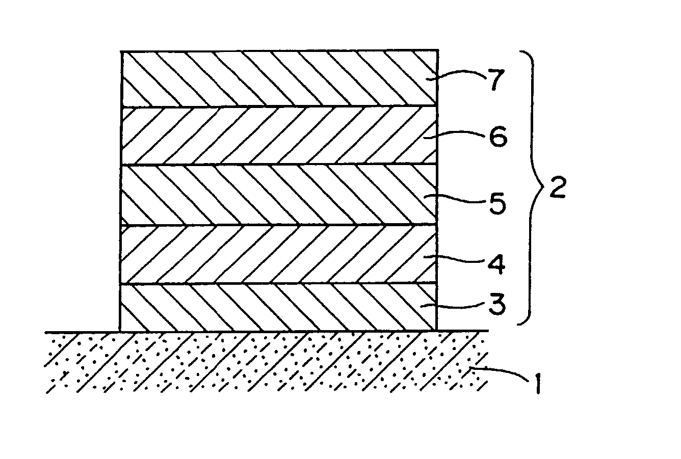
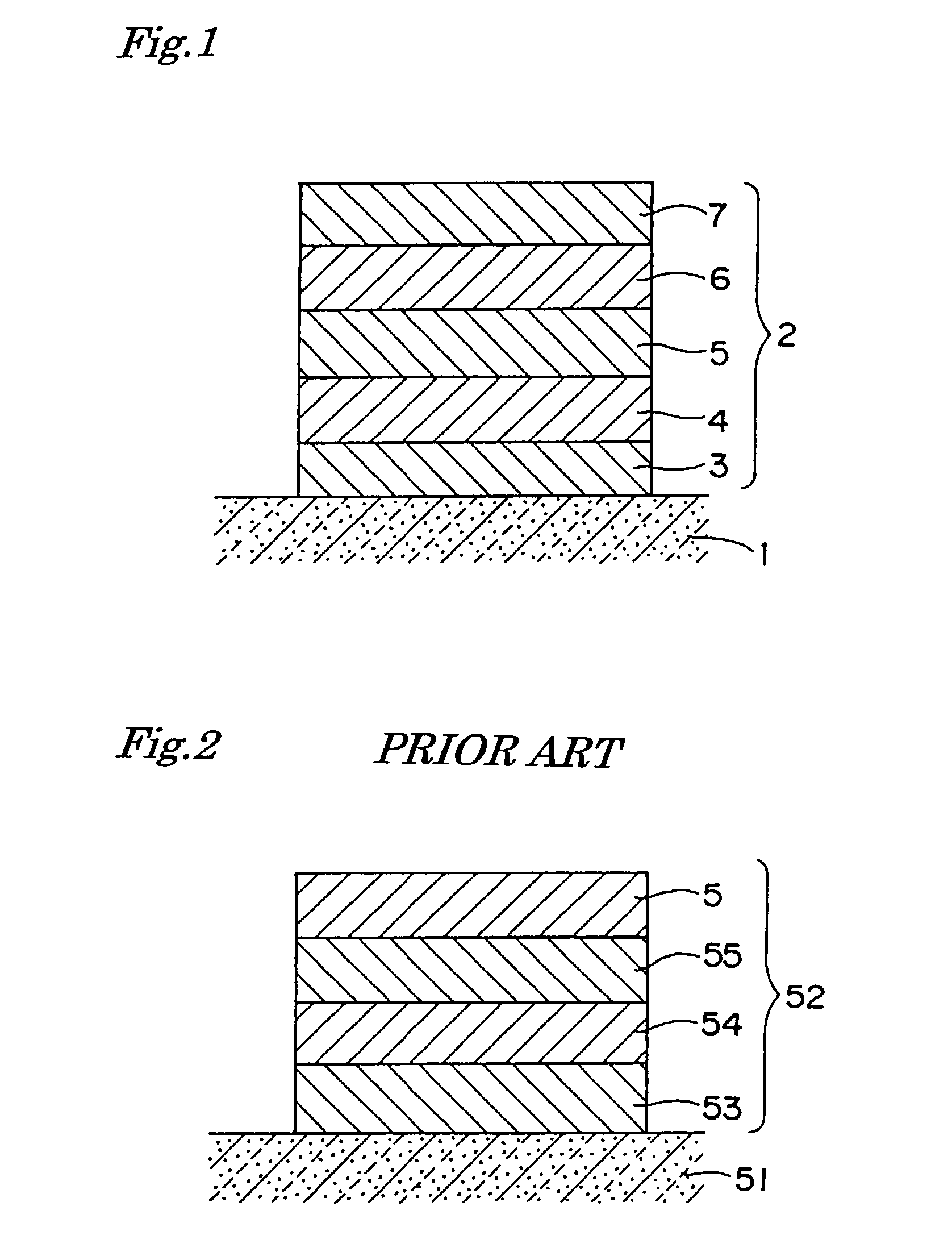
[0030] 1. Formation of the Backside Electrode

[0031] The layers of aluminum, molybdenum, nickel; silver and gold were deposited in this order on the backside of the semiconductor substrate by vacuum deposition techniques. The thickness of the layers of aluminum, molybdenum and nickel were 500 nm, 2000 nm and 300 nm, respectively. The thickness of the layers of silver and gold were changed in the range of 0 to 2000 nm and 0 to 200 nm, respectively.

[0032] 2. Evaluation of the Solderability

[0033] Solder wettability and percentage of inter layer peeling of electrode were evaluated for the semiconductor device produced by the above-mentioned method. The solder wettability was measured by mi-scope ultrasonic inspection image analyzer (available from Hitachi Kenki Corporation.) and the percentage of rejection of soldering was calculated. The percentage of inter layer peeling of electrode was measured by universal bond tester 2400 (available from Daisy Corporation.) Further, surface analysis...


PUM


Abstract

The semiconductor device has a backside electrode disposed on a backside of the semiconductor substrate and including multiple layers of metal. The backside electrode includes, on the semiconductor substrate, a first layer of aluminum, a second layer of barrier metal, a third layer of nickel, a fourth layer of silver and a fifth layer of gold which are disposed in this order.

Description

[0001] 1. Field of the Invention[0002] The present invention relates to semiconductor device having a backside electrode for solder mounting, which is formed on a back side of a p-type semiconductor substrate.[0003] 2. Description of the Prior Art[0004] The backside electrode is formed on the back side of the substrate of the semiconductor device having the p-type semiconductor substrate such as a diode, a bipolar-diode and IGBT.[0005] FIG. 2 is a schematic cross-sectional view of a part of a conventional semiconductor device. In this figure, reference numeral 51 is a p-type semiconductor substrate, and reference numeral 52 is a backside electrode formed on the p-type semiconductor substrate 51. The backside electrode 52 includes a first metal layer 53 of aluminum, a second metal layer 54 of molybdenum or titanium as a barrier metal layer, a third metal layer 54 of nickel solderable to a lead frame and the substrate and an outermost fourth metal layer of gold. First metal layer 53 o...

Claims


Application Information

Patent Timeline
IPC IPC(8): H01L21/52H01L21/28H01L23/482
CPCH01L24/32H01L2924/13055H01L2924/1305H01L23/4827H01L2924/00
Inventor UCHIDA, KIYOHIROTSUTSUMI, KEISUKE
Owner MITSUBISHI ELECTRIC CORP
Why Eureka
Try Eureka