Light emitting device, method of manufacturing the same, and manufacturing apparatus therefor

Inactive Publication Date: 2003-07-03
SEMICON ENERGY LAB CO LTD
View PDF2 Cites 117 Cited by
  • Summary
  • Abstract
  • Description
  • Claims
  • Application Information

AI Technical Summary

Problems solved by technology

However, with these methods the film formation precision is not very high.
These demands become a big problem, however, in that the pitch between pixels becomes finer along with making the light emitting device higher in definition (increasing the number of pixels) and reducing the size of the light emitting device.
There is a problem with light emitting devices in that external light (light from outside of the light emitting device) made incident to pixels which are not emitting light is reflected by rear surfaces of the cathodes (surfaces contacting the light emitting layer), and the rear surfaces of the cathodes act as a mirror, reflecting external scener

Method used


Image

  • Light emitting device, method of manufacturing the same, and manufacturing apparatus therefor
  • Light emitting device, method of manufacturing the same, and manufacturing apparatus therefor
  • Light emitting device, method of manufacturing the same, and manufacturing apparatus therefor

Examples


Example

[0115] Embodiment 1

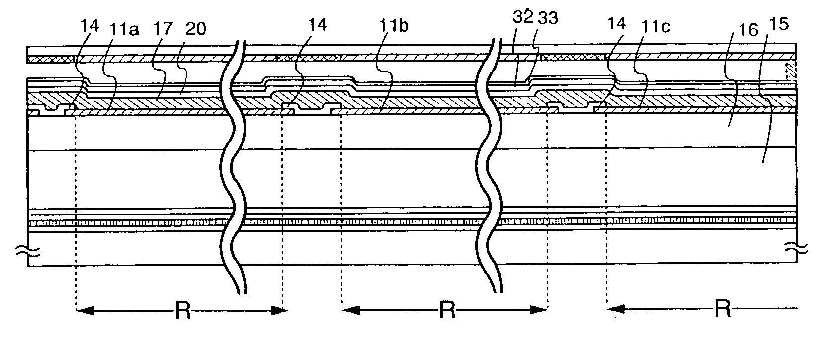
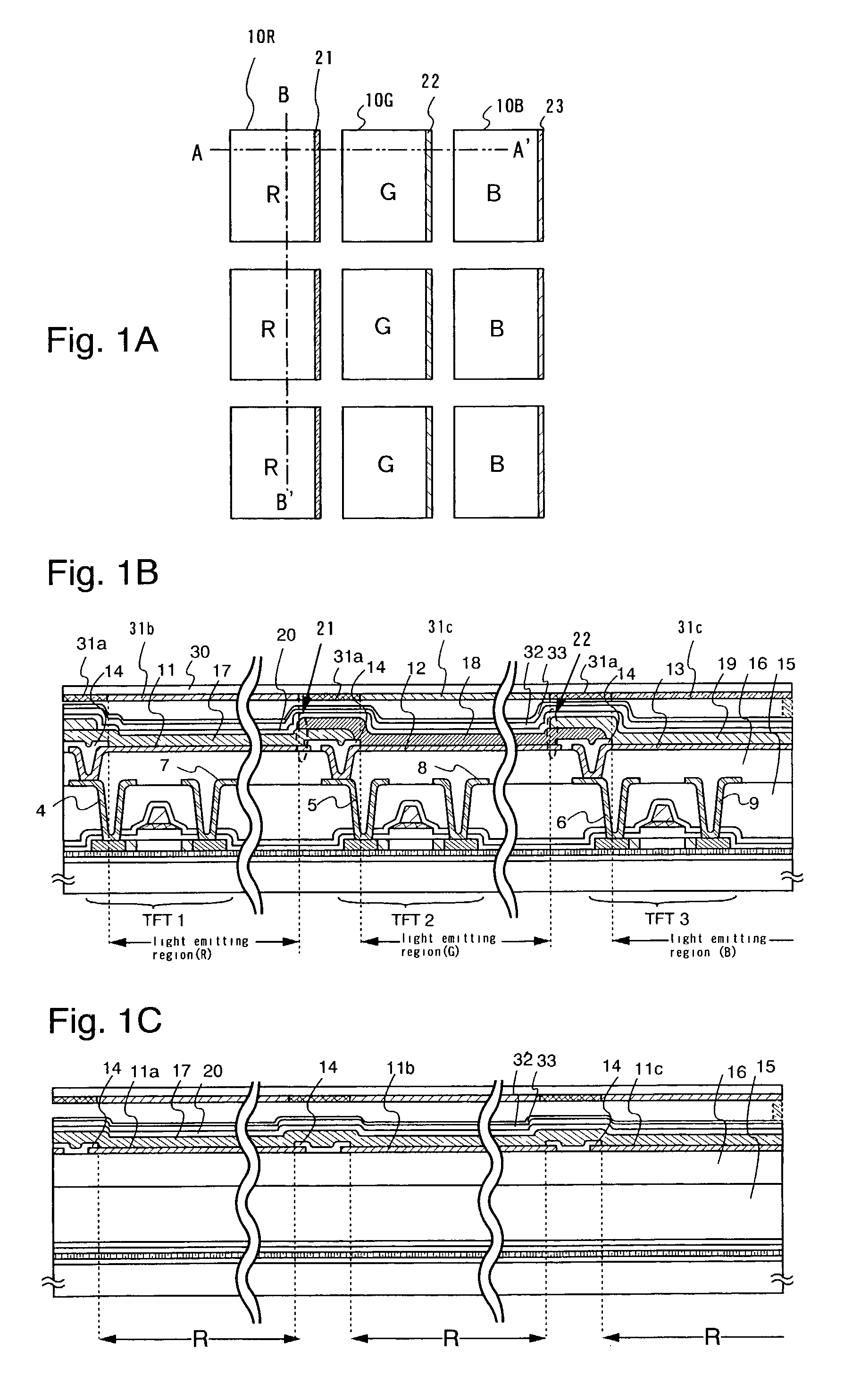
[0116] In this embodiment, an active matrix type light emitting device manufactured on an insulating film will be described. FIG. 6 is a cross sectional view of the active matrix type light emitting device. As an active element, a thin film transistor (hereafter referred to as TFT) is used here, a MOS transistor may also be used.

[0117] A top gate TFT (specifically a planar TFT) is shown as an example, a bottom gate TFT (typically inversely staggered TFT) may also be used.

[0118] In this embodiment, a substrate 800 is used, which is made of barium borosilicate glass or alumino borosilicate glass, a quartz substrate, a silicon substrate, a metal substrate, or stainless substrate forming an insulating film on the surface may be used. A plastic substrate having heat resistance enduring a treatment temperature of this embodiment also may be used, and further a flexible substrate may be used.

[0119] Next, a silicon oxynitride film is formed as a lower layer 801 of a base ...

Example

[0167] Embodiment 2

[0168] The top surface view and the cross-sectional view of the module type light emitting device (also referred to as EL module) obtained by Embodiment 1 are shown.

[0169] FIG. 7A is a view of a top surface view of EL module and FIG. 7B is a cross-sectional view taken along the line of A-A' of FIG. 7A. FIG. 7A shows that the base insulating film 401 is formed on the substrate 400 (such as a heat resistant glass, for example), and the pixel portion 402, the source side driver circuit 404, and the gate side driver circuit 403 are formed thereon. These pixel portion and driver circuit may be obtained according to above-mentioned Embodiment 1.

[0170] The reference numeral 419 is a protective film. The pixel portion and the driver circuit portion are covered by the protective film 419. In addition, the protective film may be sealed by the cover material 420 using the bonding member. A sealing substrate (such as a glass substrate and a plastic substrate) may be used as t...

Example

[0189] Embodiment 3

[0190] By implementing the present invention, EL modules (active matrix EL module and passive EC module) can be completed. Namely, by implementing the present invention, all of the electronic equipments into which the various modules are built are completed.

[0191] Following can be given as such electronic equipments: video cameras; digital cameras; head mounted displays (goggle type displays); car navigation systems; car stereos; personal computers; portable information terminals (mobile computers, mobile phones, electronic books etc.) etc. Examples of these are shown in FIGS. 9A to 9F and 10A to 10C.

[0192] FIG. 9A is a personal computer which comprises: a main body 2001; an image input section 2002; a display section 2003; and a keyboard 2004 etc.

[0193] FIG. 9B is a video camera which comprises: a main body 2101; a display section 2102; a voice input section 2103; operation switches 2104; a battery 2105 and an image receiving section 2106 etc.

[0194] FIG. 9C is a ...


PUM


Abstract

A light emitting device having high definition, a high aperture ratio, and high reliability is provided. The present invention achieves high definition and a high aperture ratio with a full color flat panel display using red, green, and blue color emission light by intentionally forming laminate portions, wherein portions of different organic compound layers of adjacent light emitting elements overlap with each other, without depending upon the method of forming the organic compound layers or the film formation precision.

Description

[0001] 1. Field of the Invention[0002] The present invention relates to a semiconductor device, in particular, the present invention relates to an organic light emitting device (OLED) having a light emitting element formed on a substrate having an insulating surface. Further, the present invention relates to an organic light emitting module on which ICs and the like, including a controller, are mounted to an organic light emitting panel. Note that the terms organic light emitting panel and organic light emitting module both refer to light emitting devices in this specification. The present invention additionally relates to an apparatus for manufacturing the light emitting device.[0003] In this specification, semiconductor devices correspond to general devices functioning by use of semiconductor characteristics. Therefore, a light emitting device, an electro-optical device, a semiconductor circuit and an electronic device are all included in the category of the semiconductor device.[...

Claims


Application Information

Patent Timeline
IPC IPC(8): H01L27/32H01L51/50H01L51/52H01L51/56H05B33/02H05B33/12H05B33/22
CPCH01L27/3218H01L51/5237H01L27/322H01L27/3281H01L21/67207H01L27/3211H01L51/56H01L2251/5315H01L51/5036H01L27/3244H01L51/5284H10K59/35H10K59/38H10K59/12H10K59/17H10K50/125H10K50/841H10K50/844H10K50/865H10K2102/3026H10K71/00H05B33/10H10K50/13H10K59/32H10K59/123H10K59/124H10K59/353H10K50/84
Inventor YAMAZAKI, SHUNPEIHAMATANI, TOSHIJITAKAYAMA, TORU
Owner SEMICON ENERGY LAB CO LTD
Why Eureka
Try Eureka