Fluorochemical treatment for silicon articles

Inactive Publication Date: 2003-12-11
3M INNOVATIVE PROPERTIES CO
View PDF36 Cites 26 Cited by
  • Summary
  • Abstract
  • Description
  • Claims
  • Application Information

AI Technical Summary

Benefits of technology

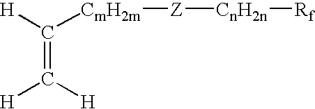
[0050] m is an integer greater than or equal to 1, desirably in the range of from about 1 to about 20, more desirably in the range of from about 1 to about 10. In some desired embodiments, m is about 1. Without wishing to be bound by theory, it is believed that the presence of one or more methylene groups (i.e., m greater than or equal to 1) provides enhanced reactivity to the fluorinated olefin as compared with electron withdrawing groups such as perfluoroalkyl or perfluoroalkylene, and provides enhanced chemical and environmental stability as compared with strong electron donating groups such as alkoxy, dialkylamino, and the like.

Problems solved by technology

The inherent mechanical nature of MEMS devices brings about a high and ever increasing level of complexity to their production and reliability.
Stiction, friction, and wear are major problems limiting both the production yield and useful lifetime of many MEMS devices, and have plagued the MEMS industry since its inception.
Such treatments typically reduce capillary forces by reducing the surface energy of MEMS surfaces (e.g., resulting in a high advancing and / or receding contact angle with water).
Many anti-stiction and / or lubrication treatments are mere liquid coatings, and thus prone to loss or removal over time.

Method used


Image

  • Fluorochemical treatment for silicon articles
  • Fluorochemical treatment for silicon articles
  • Fluorochemical treatment for silicon articles

Examples


example 12

[0147] A 0.5 cm.times.0.5 cm square silicon chip having a series of unreleased (i.e., still having a protective photoresist) MEMS cantilever beams (similar to that described in R. Maboudian et al., Tribology Letters, vol. 3, pp. 215-221 (1997), the disclosure of which is incorporated herein by reference) was made utilizing the Cronos MUMPS process with the following noted changes. The unreleased beams were made of polycrystalline silicon and positioned parallel to the polycrystalline silicon surface at a distance of 2 micrometers. The beams were regularly spaced to form an array (20 micrometers pitch), 3.5 micrometers thick, 10 micrometers wide, and had lengths varying in intervals of 50 micrometers from 200 to 1500 micrometers. The chip also had reference posts having a height of 5.5 micrometers thickness.

[0148] To remove protective photoresist resulting from the MUMPS process, the chip was sonicated in acetone for 20 min using an ultrasonic bath, obtained under the trade designati...

example 19

[0158] carried out according to General Method C, except that a polycrystalline silicon wafer (10,000 .ANG. undoped polysilicon on a 100 mm diameter Si(100) wafer obtained from WaferNet; prepared according to General Procedure A with the exception that the wafer piece was etched in CMOS grade 49 percent by weight aqueous HF for 3 min instead of etching in the ammonium fluoride solution) was used as the substrate, and E1 was used at 45 weight percent in a mixture of 5 weight percent 2-hydroxy-2-methyl-1-phenyl-1-propanone and 50 weight percent heptane.

[0159] Example 20 was carried out as in Example 19 except that E1 was used at 5 weight percent in a mixture of 5 weight percent 2-hydroxy-2-methyl-1-phenyl-1-propanone and 90 weight percent heptane.

[0160] Example 21 was carried out using a 1.times.1 cm piece of silicon (100) (obtained from WaferNet). The piece was cleaned by sequentially rinsing it in heptane, acetone, and isopropyl alcohol. The cleaned piece was subjected for 10 min to...

example 22

[0165] A silicon chip, prepared as in Example 12, containing MEMS cantilever beams and having the photoresist removed, was placed in the "fill / drain" apparatus. A volume of 5 mL CMOS grade 49 percent by weight aqueous HF was added to the apparatus and allowed to etch the chip for 3 min to release the cantilever beam MEMS devices. The chip was then washed with 10.times.25 mL portions of deionized water (.gtoreq.18 megohms resistance) over a total period of 10 min. After the last of the water was drained, 5 mL of CMOS grade 49 percent by weight aqueous HF was added and allowed to etch the MEMS chip again for 3 min. The aqueous HF was again drained. The etched chip was then sequentially washed in isopropyl alcohol for 10 min, and heptane for 10 min, each wash being performed in the same manner as the water wash, with 10 fill and drain cycles over 10 min.

[0166] The chip was removed from the heptane, and placed in a quartz tube in a solution (sparged with dry nitrogen for 15 min) contain...


PUM

PropertyMeasurementUnit
Percent by massaaaaaaaaaa
Angleaaaaaaaaaa

Abstract

Silicon substrates having Si-H bonds are chemically modified using a fluorinated olefin having the formula: wherein m is an integer greater than or equal to 1; n is an integer greater than or equal to 0; Z is a divalent linking group; and Rf is a highly fluorinated organic group.

Description

[0001] The present invention relates generally to chemical modification of silicon substrates, and more specifically to chemical modification of silicon-based microelectromechanical systems (i.e., MEMS) devices.[0002] MEMS devices are used, for example, as airbag accelerometers, microengines, optical switches, gyroscopic devices, sensors, and actuators. MEMS devices are typically manufactured from a silicon wafer using microlithography, and have freestanding active silicon elements (e.g., gears, hinges, levers, slides, and mirrors) that must be free to move, rotate, etc. The inherent mechanical nature of MEMS devices brings about a high and ever increasing level of complexity to their production and reliability.[0003] MEMS devices generally have large surface-area-to-volume ratios, and thus their performance is often dominated by strong adhesion (i.e., stiction) of active silicon elements to one another and / or to the supporting silicon substrate. Stiction may be caused by capillary ...

Claims


Application Information

Patent Timeline
IPC IPC(8): B81B3/00B81C1/00
CPCB81B3/0005B82Y30/00B81C1/0096
Inventor DUNBAR, TIMOTHY D.ZAZZERA, LAWRENCE A.PELLERITE, MARK J.BOARDMAN, LARRY D.MOORE, GEORGE G.GUERRA, MIGUEL A.ELSBERND, CHERYL L.
Owner 3M INNOVATIVE PROPERTIES CO
Why Eureka
Try Eureka