Optical recording medium
- Summary
- Abstract
- Description
- Claims
- Application Information
AI Technical Summary
Benefits of technology
Problems solved by technology
Method used
Image
Examples
working example 1
[0147] An optical recording medium sample was fabricated in the following manner.
[0148] A disk-like polycarbonate substrate having a thickness of 1.1 mm and a diameter of 120 mm was first fabricated by an injection molding process. No grooves or lands were formed on the surface of the polycarbonate substrate.
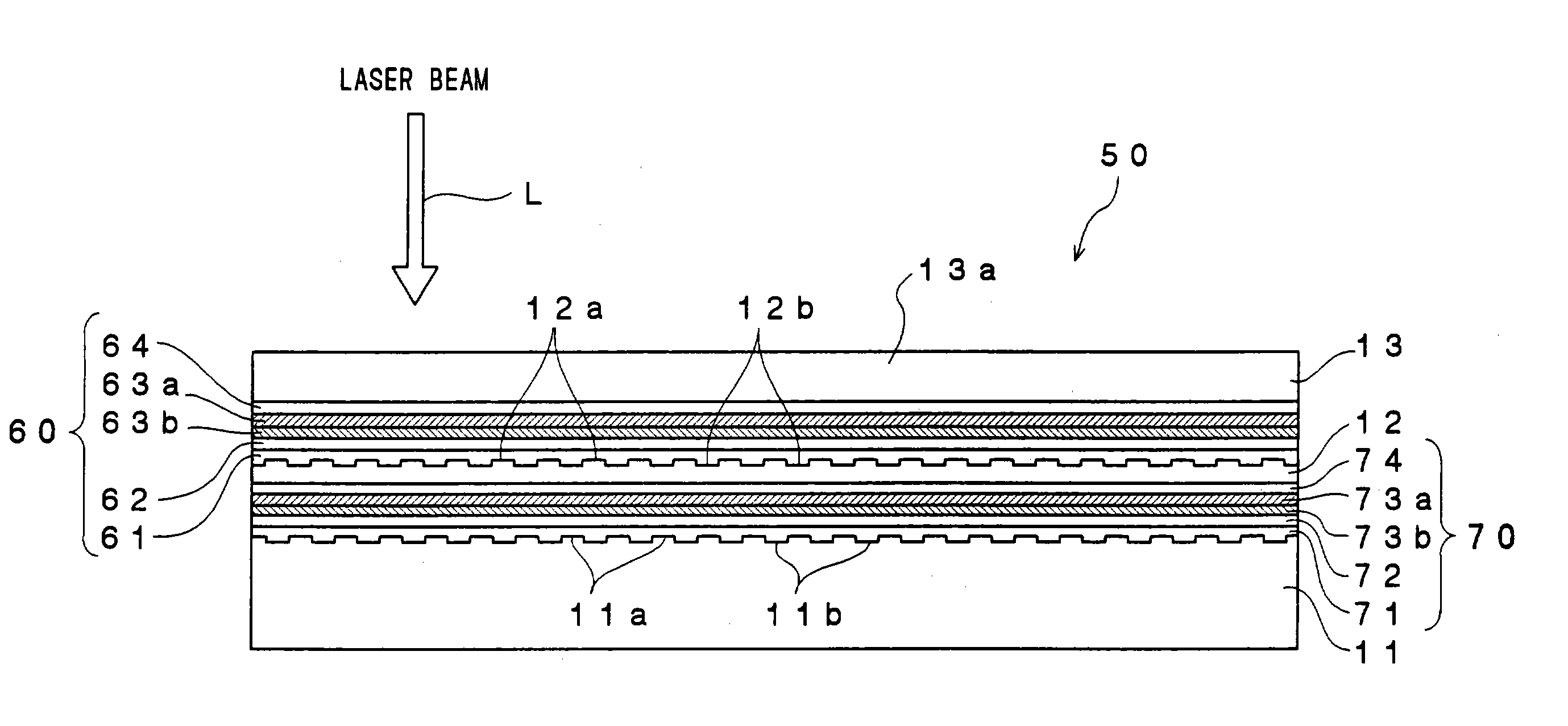
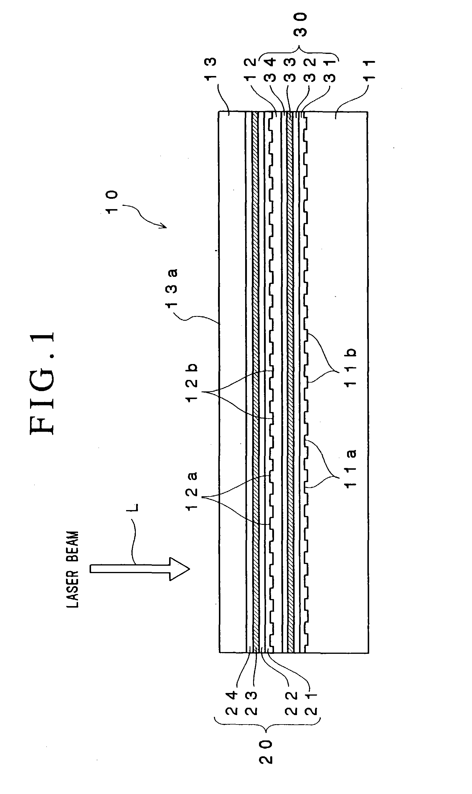
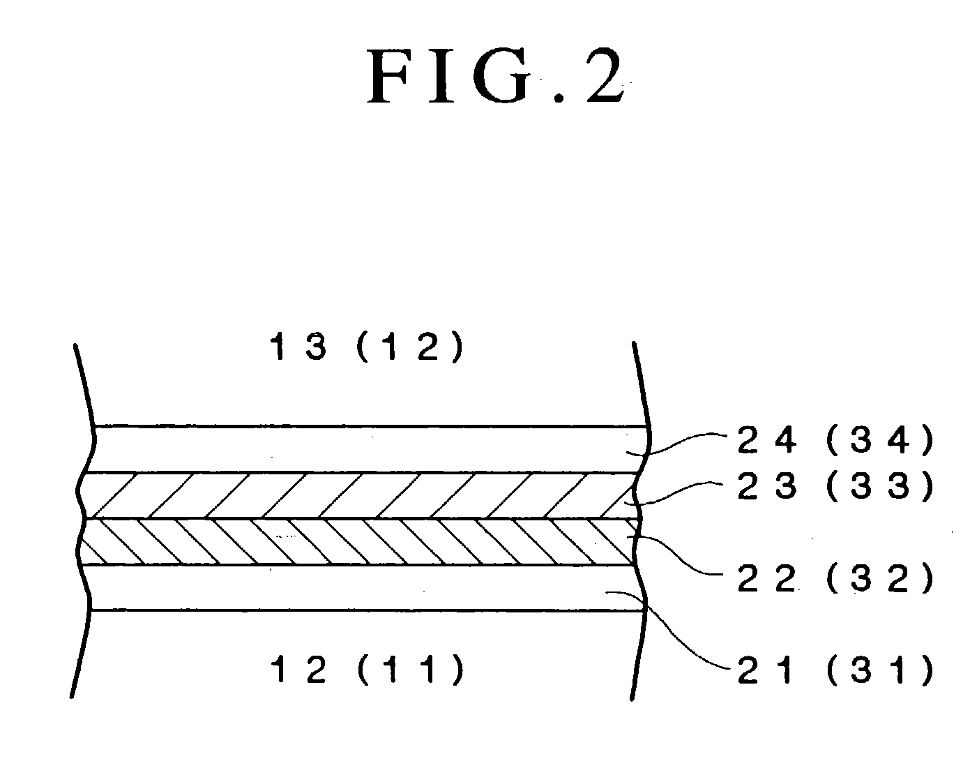
[0149] Then, the polycarbonate substrate was set on a sputtering apparatus and a reflective film containing Ag as a primary component and C as an additive and having a thickness of 8 nm, a second dielectric film containing a mixture of ZnS and SiO.sub.2 and having a thickness of 32 nm, a second recording film containing Si as a primary component and having a thickness of 5 nm, a first recording film containing Cu as a primary component and having a thickness of 5 nm and a first dielectric film containing the mixture of. ZnS and SiO.sub.2 and having a thickness of 30 nm were sequentially formed on the polycarbonate substrate using the sputtering process.
[0150] Further, the first ...
working example 2
[0156] Samples were fabricated in the following manner.
[0157] A disk-like polycarbonate substrate having a thickness of 1.1 mm and a diameter of 120 mm was first fabricated by an injection molding process. No grooves or lands were formed on the surface of the polycarbonate substrate.
[0158] Then, the polycarbonate substrate was set on a sputtering apparatus and a reflective film containing Ag as a primary component and C as an additive and having a thickness of 100 nm was formed on the polycarbonate substrate using the sputtering process.
[0159] In this manner, six samples were fabricated with varying amounts of C added to the reflective film.
[0160] The reflective film of each of the thus fabricated samples was irradiated with a laser beam having a wavelength of 405 nm and the amount of the laser beam reflected by the reflective film was detected, thereby measuring the reflection coefficient Rco of the reflective film of the sample.
[0161] Further, each of the samples was held at a tem...
working example 3
[0166] Samples were fabricated in the following manner.
[0167] A disk-like polycarbonate substrate having a thickness of 1.1 mm and a diameter of 120 mm was first fabricated by an injection molding process. No grooves or lands were formed on the surface of the polycarbonate substrate.
[0168] Then, the polycarbonate substrate was set on a sputtering apparatus and a reflective film containing Ag as a primary component and 2.5 atomic % of C as an additive and having a thickness of 100 nm was formed on the polycarbonate substrate using the sputtering process, thereby fabricating a sample #1.
[0169] A similarly fabricated polycarbonate substrate was set on a sputtering apparatus and a reflective film containing Ag as a primary component and 5.0 atomic % of C as an additive and having a thickness of 100 nm was formed on the polycarbonate substrate using the sputtering process, thereby fabricating a sample # 2.
[0170] A similarly fabricated polycarbonate substrate fabricated similarly was set ...
PUM
 Abstract
Description
Claims
Application Information


