
Plasma processes for depositing low dielectric constant films

a dielectric constant film and plasma technology, applied in the direction of centrifugal wheel fertilisers, applications, transportation and packaging, etc., can solve the problems of affecting the overall performance of the device, affecting the device structure, and inadequate etch stop layer material

Inactive Publication Date: 2004-02-26
APPLIED MATERIALS INC
View PDF50 Cites 15 Cited by
  • Summary
  • Abstract
  • Description
  • Claims
  • Application Information

AI Technical Summary

Problems solved by technology

The high temperatures at which some thermal CVD processes operate can damage device structures having layers previously formed on the substrate.
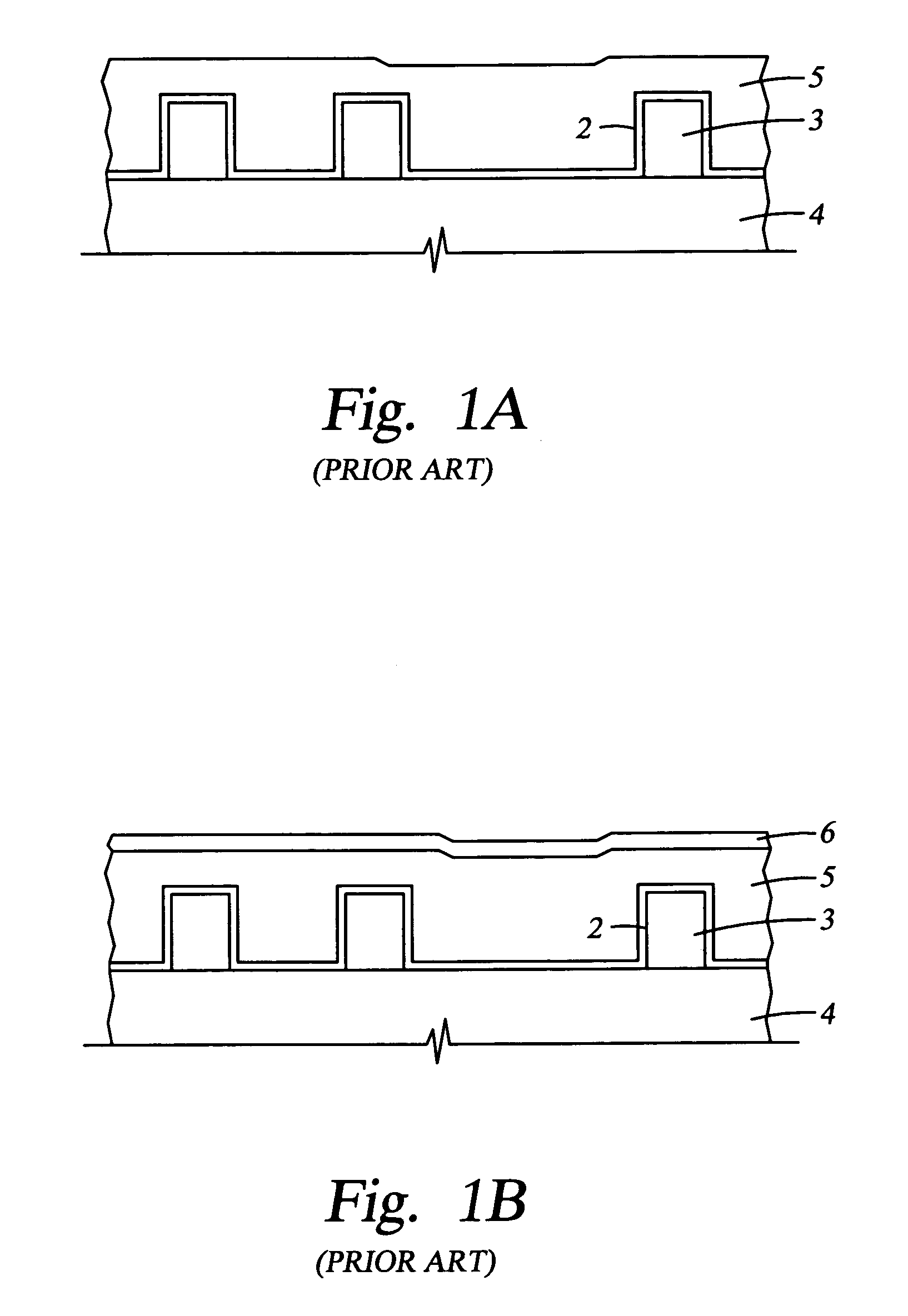
However, the barrier / liner layers typically have dielectric constants that are significantly greater than 4.0, and the high dielectric constants result in a combined insulator that does not significantly reduce the dielectric constant.
Furthermore, known low k dielectric materials generally have low oxide content which makes the material inadequate as an etch stop layer during etching of vias and / or interconnects.
This may lead to crosstalk and / or resistance-capacitance (RC) delay that degrades the overall performance of the device.
The '570 patent does not identify process conditions for making barrier layers having low dielectric constants or for making etch stop layers having high oxide contents.
Gap filling layers produced from methylsilane are typically hydrophilic and have poor moisture barrier properties.

Method used


Image

  • Plasma processes for depositing low dielectric constant films
  • Plasma processes for depositing low dielectric constant films
  • Plasma processes for depositing low dielectric constant films

Examples


Embodiment Construction

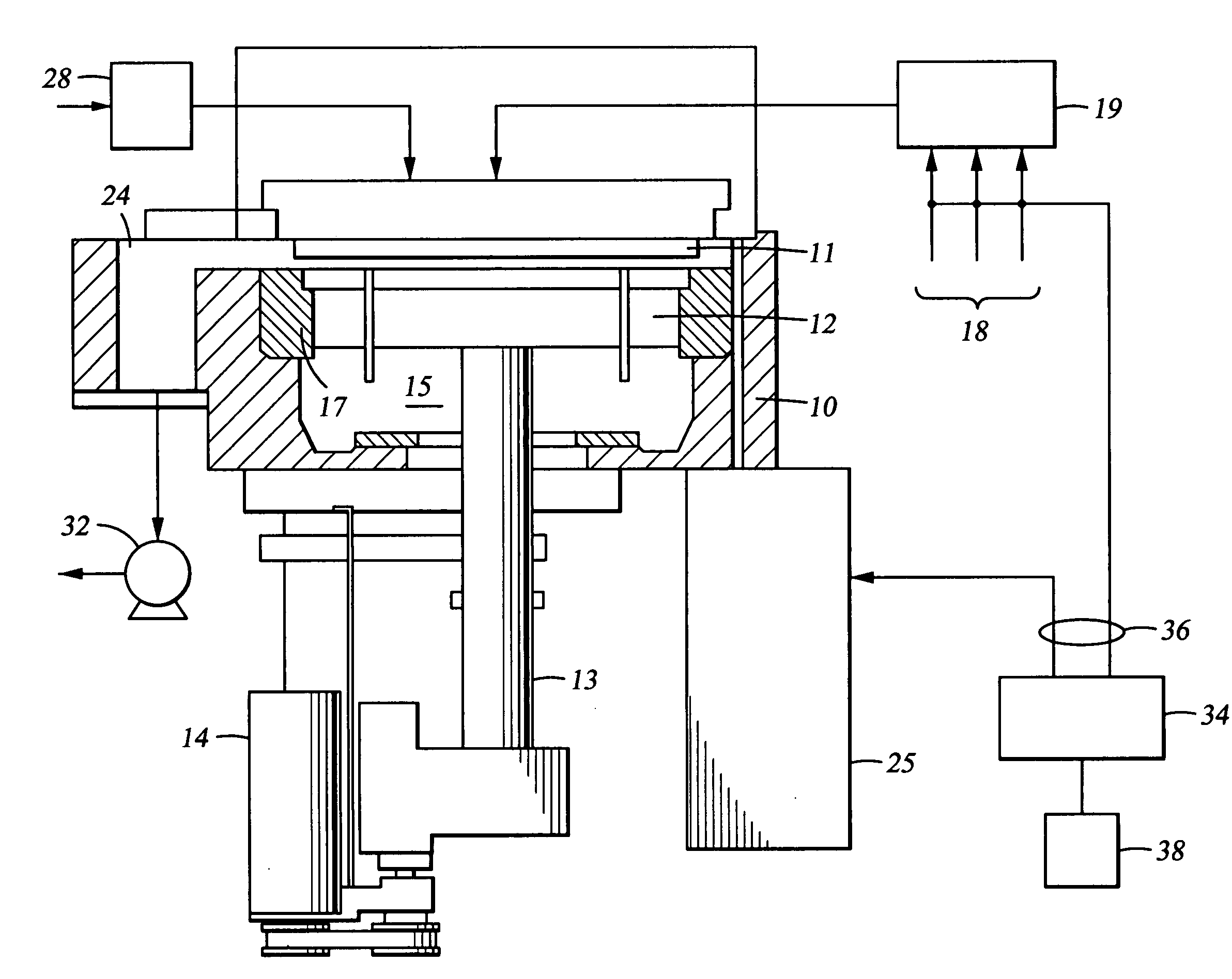
[0111] The following example and demonstrates deposition of an oxidized organosilane or organosiloxane film having excellent barrier and adhesion properties. This example was undertaken using a chemical vapor deposition chamber, and in particular, a "CENTURA DxZ" system which includes a solid-state RF matching unit with a two-piece quartz process kit, both fabricated and sold by Applied Materials, Inc., Santa Clara, Calif.

[0112] Non-Pulsed RF Power

[0113] An oxidized dimethylsilane film was deposited at a chamber pressure of 3.0 Torr and temperature of 15 EC from reactive gases which were flowed into the reactor as follows:

4 Dimethylsilane, (CH.sub.3).sub.2SiH.sub.2, at 55 sccm Nitrous oxide, N.sub.2O, at 300 sccm Helium, He, at 4000 sccm.

[0114] The substrate was positioned 600 mil from the gas distribution showerhead and 20 W of high frequency power (13 MHz) was applied to the showerhead for plasma enhanced deposition of an oxidized dimethylsilane layer. The oxidized dimethylsilane ...


PUM

PropertyMeasurementUnit
sizesaaaaaaaaaa
sizesaaaaaaaaaa
pressuresaaaaaaaaaa

Abstract

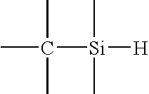
A method and apparatus for depositing a low dielectric constant film by reaction of an organosilicon compound and an oxidizing gas at a constant RF power level from about 10W to about 200W or a pulsed RF power level from about 20W to about 500W. Dissociation of the oxidizing gas can be increased prior to mixing with the organosilicon compound, preferably within a separate microwave chamber, to assist in controlling the carbon content of the deposited film. The oxidized organosilane or organosiloxane film has good barrier properties for use as a liner or cap layer adjacent other dielectric layers. The oxidized organosilane or organosiloxane film may also be used as an etch stop and an intermetal dielectric layer for fabricating dual damascene structures. The oxidized organosilane or organosiloxane films also provide excellent adhesion between different dielectric layers. A preferred oxidized organosilane film is produced by reaction of methylsilane, CH3SiH3, dimethylsilane, (CH3)2SiH2, or 1,1,3,3-tetramethyl-disiloxane, (CH3)2-SiH-O-SiH-(CH3)2, and nitrous oxide, N2O, at a constant RF power level from about 10W to about 150W, or a pulsed RF power level from about 20W to about 250W during 10% to 30% of the duty cycle.

Description

[0001] This application is a continuation of co-pending U.S. patent application Ser. No. 09 / 957,551, which was filed on Sep. 19, 2001, which is a continuation of co-pending U.S. patent application Ser. No. 09 / 247,381 [AMAT / 2592.P2], which was filed on Feb. 10, 1999, now issued as U.S. Pat. No. 6,348,725, which is a continuation-in-part of co-pending U.S. patent application Ser. No. 09 / 021,788 [AMAT / 2592], which was filed on Feb. 11, 1998, now issued as U.S. Pat. No. 6,054,379, a continuation in part of co-pending U.S. patent application Ser. No. 09 / 114,682 [AMAT / 2592.01], which was filed on Jul. 13, 1998, now issued as U.S. Pat. No. 6,072,227, a continuation-in-part of co-pending U.S. patent application Ser. No. 09 / 162,915 [AMAT / 3032], which was filed on Sep. 29, 1998, now issued as U.S. Pat. No. 6,287,990; and a continuation-in-part of co-pending U.S. patent application Ser. No. 09 / 185,555 [AMAT / 3032.P1], which was filed on Nov. 4,1998, now issued as U.S. Pat. No. 6,303,523.[0002] ...

Claims


Application Information

Patent Timeline
Patent Type & Authority Applications(United States)
IPC IPC(8): A01C15/02A01C17/00C23C16/40H01L21/316H01L21/768
CPCC23C16/401H01L2221/1031H01L21/02203H01L21/02208H01L21/02274H01L21/0228H01L21/02304H01L21/02362H01L21/31612H01L21/76801H01L21/76808H01L21/7681H01L21/76829H01L21/76832H01L21/76834H01L21/76835H01L21/02126Y10T428/31663H01L21/02211H01L21/02216H01L21/02271
Inventor CHEUNG, DAVIDYAU, WAI-FANMANDAL, ROBERT P.JENG, SHIN-PUULIU, KUO-WEILU, YUNG-CHENGBARNES, MICHAELWILLECKE, RALF B.MOGHADAM, FARHADISHIKAWAPOON, TZE WING
Owner APPLIED MATERIALS INC
Learn More