Nickel silicide - silicon nitride adhesion through surface passivation

Inactive Publication Date: 2004-04-01
TEXAS INSTR INC
View PDF5 Cites 17 Cited by
  • Summary
  • Abstract
  • Description
  • Claims
  • Application Information

AI Technical Summary

Problems solved by technology

One technical challenge to the engineers in their endeavor to reduce the silicon integrated circuit component size is to maintain the conductance of the conductive lines that hook up the circuit components.
But cobalt silicide process encounters problems when polysilicon line becomes narrower than 50 nanometers.
One problem is that cobalt silicide requires a temperature of about 700.degree. C. to form, which over taxes the thermal budget of total process.
Another problem is at 700.degree. C., grains in the polysilicon conglomerate, which reduces the polysilicon volume and causes the formation of voids in the polysilicon lines.
There are problems, however, that keep the nickel silicide clad polysilicon process from widely implemented.
One known problem is that the insu

Method used


Image

  • Nickel silicide - silicon nitride adhesion through surface passivation
  • Nickel silicide - silicon nitride adhesion through surface passivation
  • Nickel silicide - silicon nitride adhesion through surface passivation

Examples


Example

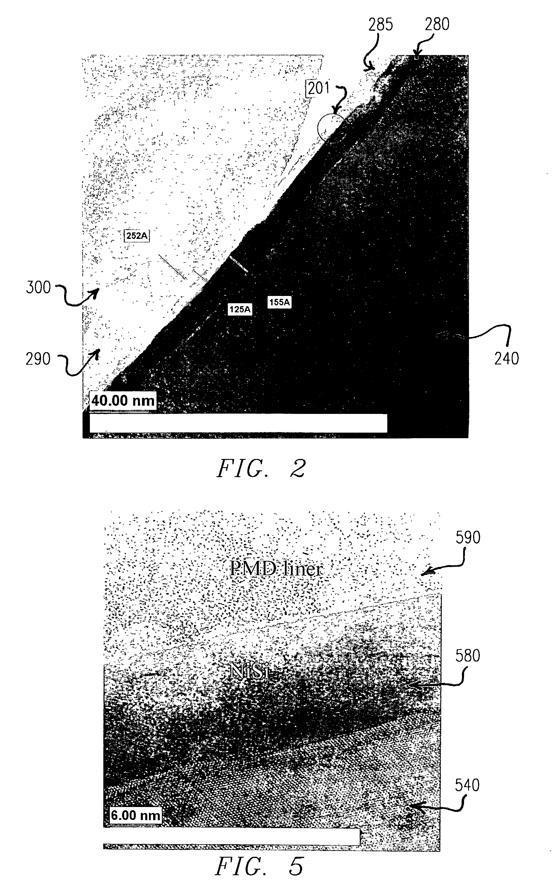
[0034] nIn the first embodiment, a nickel silicide is provided on the silicon substrate with the two-step heat-treatment process as described above. In order to prevent the silicon rich layer 285 as shown in FIG. 2 from forming, a process step is added to the silicon nitride deposition process. In this step, ammonia or other nitrogen carrying gaseous material such as nitrogen gas is introduced into the plasma reactor chamber. The gaseous atmosphere in the reactor chamber is substantially free of silicon species. Plasma is then induced by the application of a radio frequency signal that in term activates the nitrogen carrying gaseous material such as ammonia. The active nitrogen species reacts with the nickel silicide surface and passivates the nickel silicide surface.

[0035] With the nickel silicide surface thus passivated, silicon nitride deposition may continue as described above. The silicon nitride deposition may be carried out in the same plasma reactor chamber or in a separate ...

Example

[0036] In the second embodiment, the first step of the two-step silicidation heat-treatment process is performed as described, that is, heat-treat the substrate at 260 to 310.degree. C. to form a nickel rich alloy at source, drain and polysilicon line regions and the residual nickel is removed. Before the second step of silicidation, a metal nitride film such as titanium nitride is disposed on the substrate, covering the nickel silicide. The second step of the heat treatment is then performed at 400 to 550.degree. C. to convert the nickel rich alloy to a nickel mono-silicide alloy. During the second step of heat treatment, the nitrogen from the metal nitride film gets incorporated in the nickel silicide surface and thus passivates the nickel silicide. The titanium nitride film is subsequently removed from the surface of the substrate before the silicon nitride film deposition.

[0037] This invention is applicable to integrated circuits manufactured on substrates other than silicon, fo...


PUM


Abstract

A process for forming nickel silicide and silicon nitride structure in a semiconductor integrated circuit device is described. Good adhesion between the nickel silicide and the silicon nitride is accomplished by passivating the nickel suicide surface with nitrogen. The passivation may be performed by treating the nickel silicide surface with plasma activated nitrogen species. An alternative passivation method is to cover the nickel silicide with a film of metal nitride and heat the substrate to about 500° C. Another alternative method is to sputter deposit silicon nitride on top of nickel silicide.

Description

[0001] This invention relates to the field of semiconductor integrated devices, and particularly relates to a process of surface passivation for improving adhesion between a nickel silicide layer and a silicon nitride layer.DESCRIPTION OF THE RELATED ART[0002] The performance of a silicon integrated circuit is related to its component size. Small components enable more integrated functionality and faster operation. One technical challenge to the engineers in their endeavor to reduce the silicon integrated circuit component size is to maintain the conductance of the conductive lines that hook up the circuit components. One type of conductive line currently used in the silicon integrated circuit industry is refractory metal silicide clad silicon. For example, cobalt silicide clad silicon is the material of choice in making MOS transistor gate electrodes and the source and drain region of high-performance logic circuits.[0003] Cobalt silicide clad silicon served its designed purpose we...

Claims


Application Information

Patent Timeline
IPC IPC(8): H01L21/28H01L21/285H01L21/318H01L21/3205H01L21/321H01L21/336H01L21/768H01L23/52H01L23/522H01L29/78H01L29/786
CPCH01L21/28052H01L21/28518H01L21/3185H01L29/665H01L21/3211H01L21/76834H01L21/321H01L21/0217
Inventor LU, JIONG-PINGTESSMER, GLENN J.HEWSON, MELISSA M.MILES, DONALD S.WILLECKE, RALF B.MCKERROW, ANDREW J.KIRKPATRICK, BRIAN K.MONTGOMERY, CLINTON L.
Owner TEXAS INSTR INC
Why Eureka
Try Eureka