Thermally-assisted magnetic writing using an oxide layer and current-induced heating

a technology of magnetic writing and oxide layer, which is applied in the field of current-induced heating in magnetic random access memory devices, can solve the problems of limited scalability beyond the 65 nm technology node, unsuitable replacement for volatile memories such as dram or sram, and very slow flash speed

Inactive Publication Date: 2004-05-20
GLOBALFOUNDRIES US INC
View PDF4 Cites 43 Cited by
  • Summary
  • Abstract
  • Description
  • Claims
  • Application Information

AI Technical Summary

Problems solved by technology

Unfortunately, Flash is very slow and has a very limited number of write cycles (about 10.sup.6) before failure, making it unsuitable as a replacement for volatile memories such as DRAM or SRAM.
It is also believed to have limited scalability beyond the 65 nm technology node.

Method used


Image

  • Thermally-assisted magnetic writing using an oxide layer and current-induced heating
  • Thermally-assisted magnetic writing using an oxide layer and current-induced heating
  • Thermally-assisted magnetic writing using an oxide layer and current-induced heating

Examples


Embodiment Construction

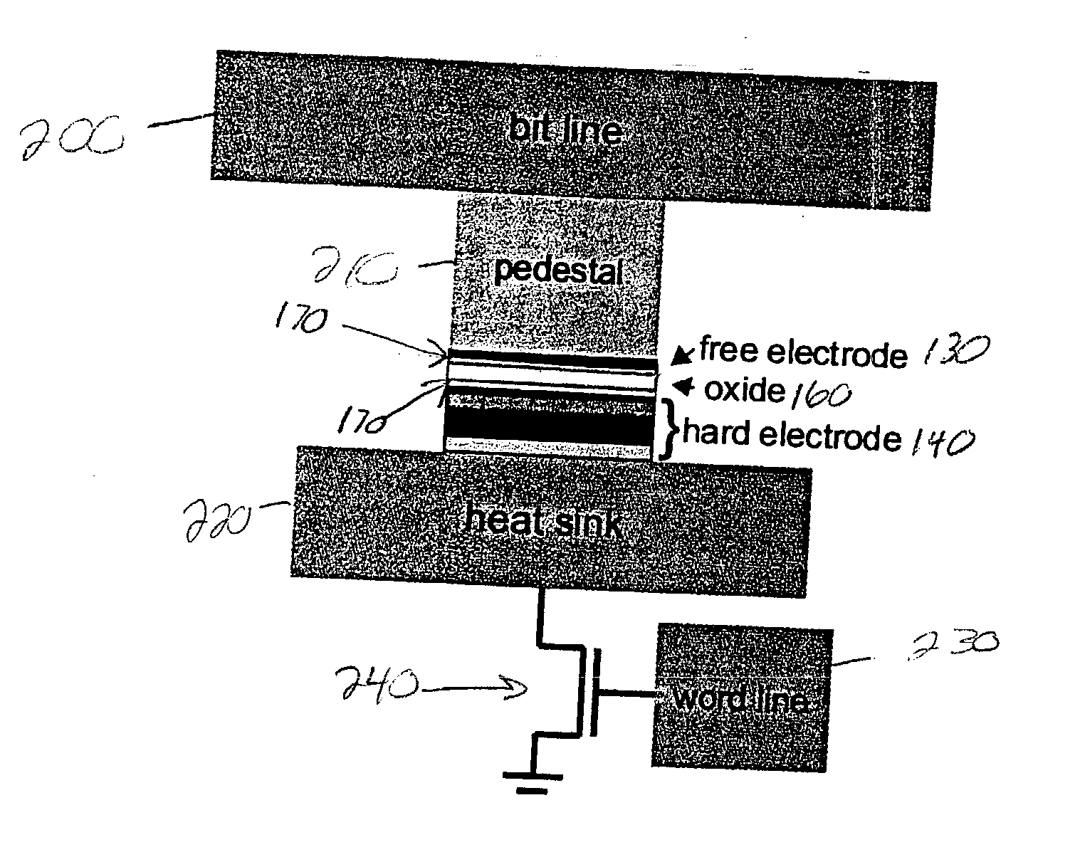
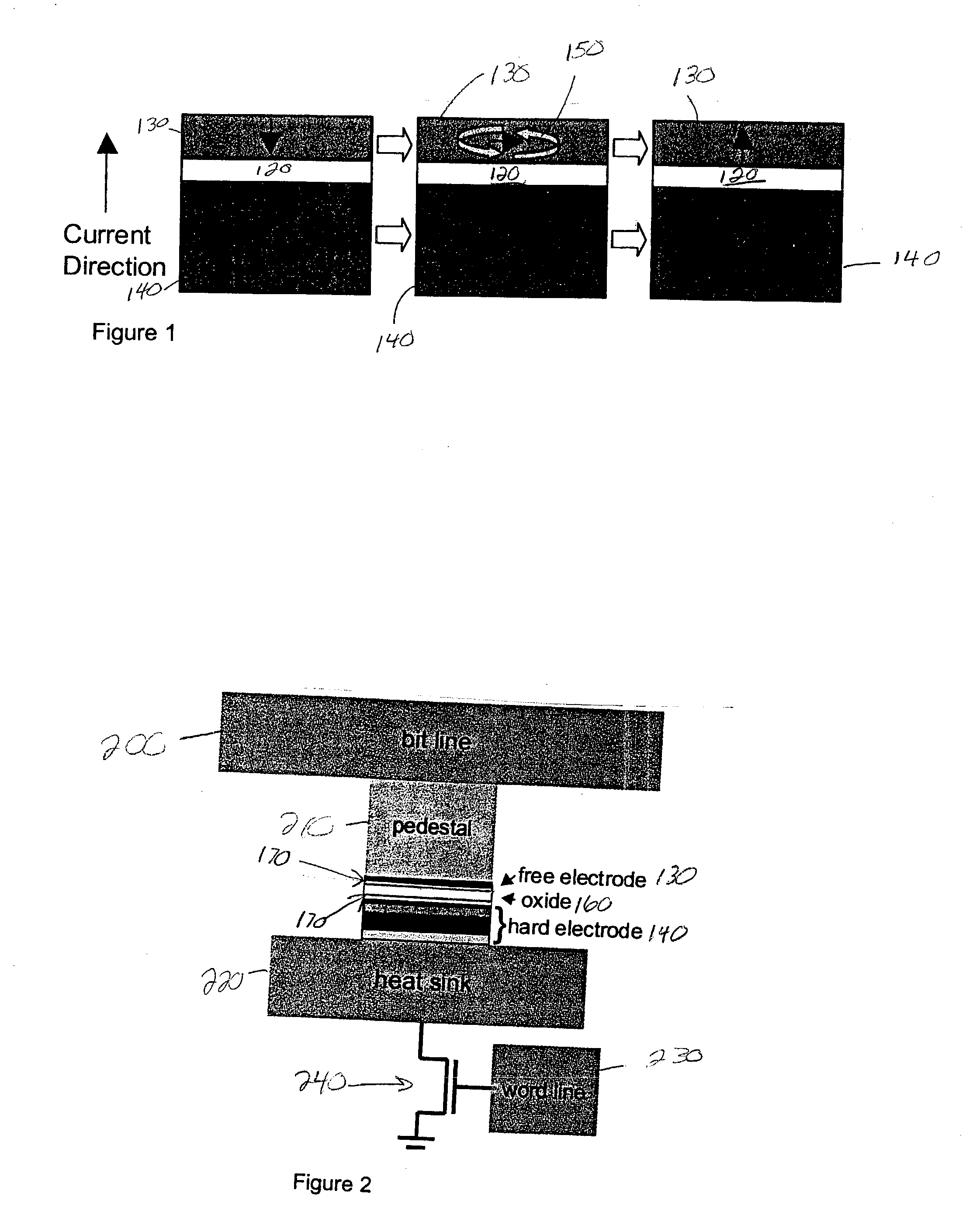
[0012] With the invention, thermally-assisted magnetic writing is accomplished by passing current through an ultra-low resistance oxide layer adjacent or near to a free electrode to be switched. Current-induced heating lowers the anisotropy of the free electrode and reduces the current density required for field or spin-transfer-based writing. In one embodiment of the invention, the resistance through the oxide layer in on the order 4 .OMEGA.-.mu.m.sup.2, the free electrode is comprising of Tb.sub.xFe.sub.y based alloy, and switching is induced by spin-transfer torque with thermal assist. Thus, the invention provides a non-volatile MRAM memory device with a large number of read and write cycles, current-controlled switching, excellent scalability, ultra-fast switching speeds, very small bit cell, low voltage, low power, and optimal resistance for CMOS integration.

[0013] As mentioned above, the non-volatile memory chip market is today dominated by Flash technology. Unfortunately, Fla...


PUM

PropertyMeasurementUnit
melting temperatureaaaaaaaaaa
resistanceaaaaaaaaaa

Abstract

A method and structure for a non-volatile magnetic random access memory (MRAM) device that has a stable magnetic electrode, an oxide layer adjacent the stable magnetic electrode, and a free magnetic electrode. The oxide layer is between the stable magnetic electrode and the free magnetic electrode. In the invention, a conductor is connected to a stable magnetic electrode. The oxide layer has a resistance at levels to allow sufficient power dissipation to lower the anisotropy of the free magnetic electrode through current induced heating. Current-induced heating is used in combination with spin-transfer torque or a magnetic field to switch the free magnetic electrode.

Description

[0001] 1. Field of the Invention[0002] The present invention generally relates to thermally-assisted magnetic writing and more particularly to current-induced heating in magnetic random access memory devices.[0003] 2. Description of the Related Art[0004] The non-volatile memory chip market is today dominated by Flash technology. Unfortunately, Flash is very slow and has a very limited number of write cycles (about 10.sup.6) before failure, making it unsuitable as a replacement for volatile memories such as DRAM or SRAM. It is also believed to have limited scalability beyond the 65 nm technology node. Therefore, there is a need for a new type of non-volatile memory.[0005] The invention provides a non-volatile magnetic random access memory (MRAM) device that has a stable magnetic electrode comprising of one or more layers, an oxide layer, and a free magnetic electrode comprising of one or more layers. When the oxide is used as a barrier, the stable and free magnetic electrodes are adj...

Claims


Application Information

Patent Timeline
Patent Type & Authority Applications(United States)
IPC IPC(8): G11C11/15H01F10/32H01F41/30H01L21/8246H01L27/105H01L27/22H01L43/08
CPCB82Y10/00B82Y25/00G11C11/15H01L43/08H01F41/305H01L27/228H01F10/3254G11C11/1675H10B61/22H10N50/10
Inventor STIPE, BARRY C.
Owner GLOBALFOUNDRIES US INC
Why Eureka
Try Eureka