Vacuum process system
- Summary
- Abstract
- Description
- Claims
- Application Information
AI Technical Summary
Benefits of technology
Problems solved by technology
Method used
Image

Examples
first embodiment
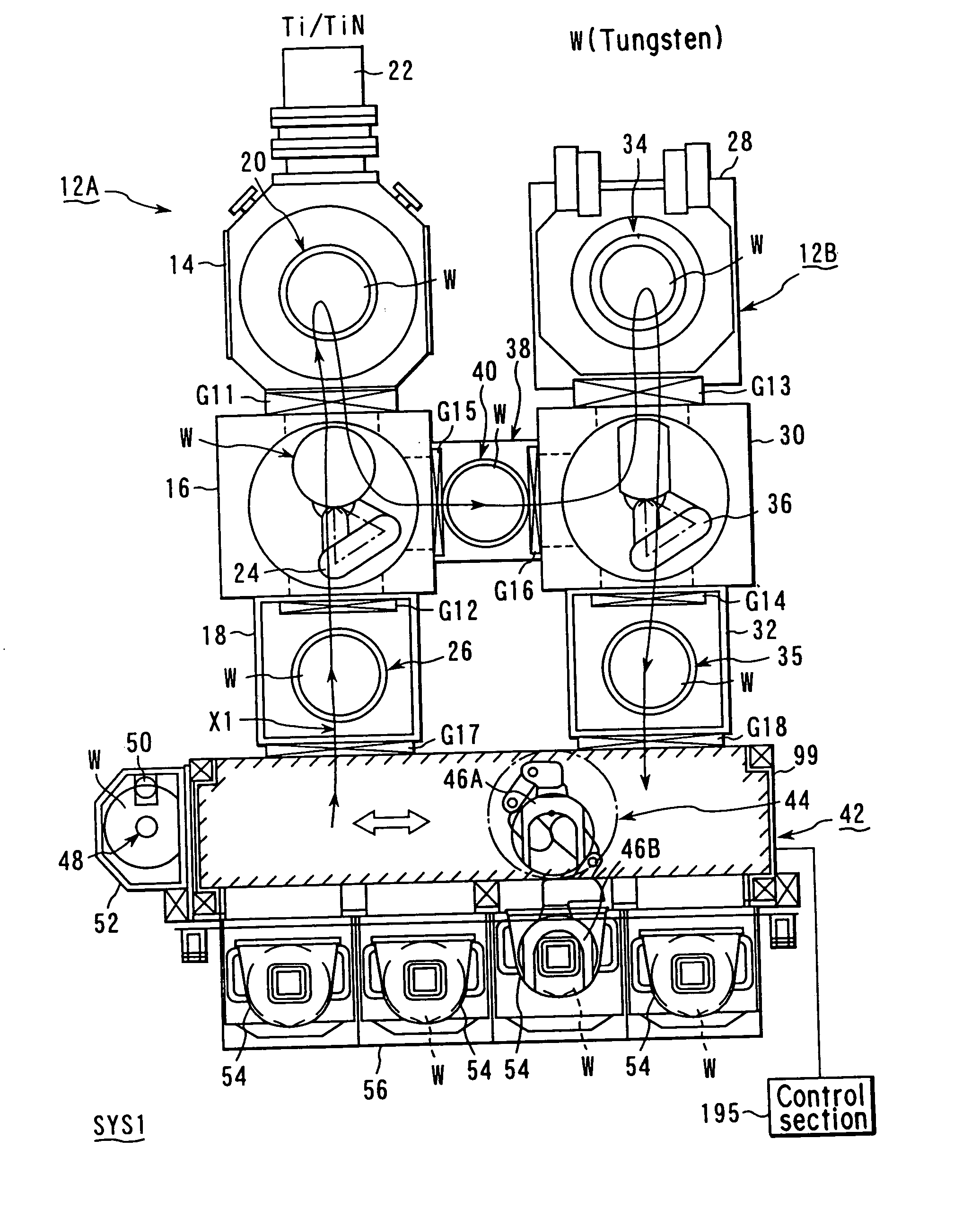
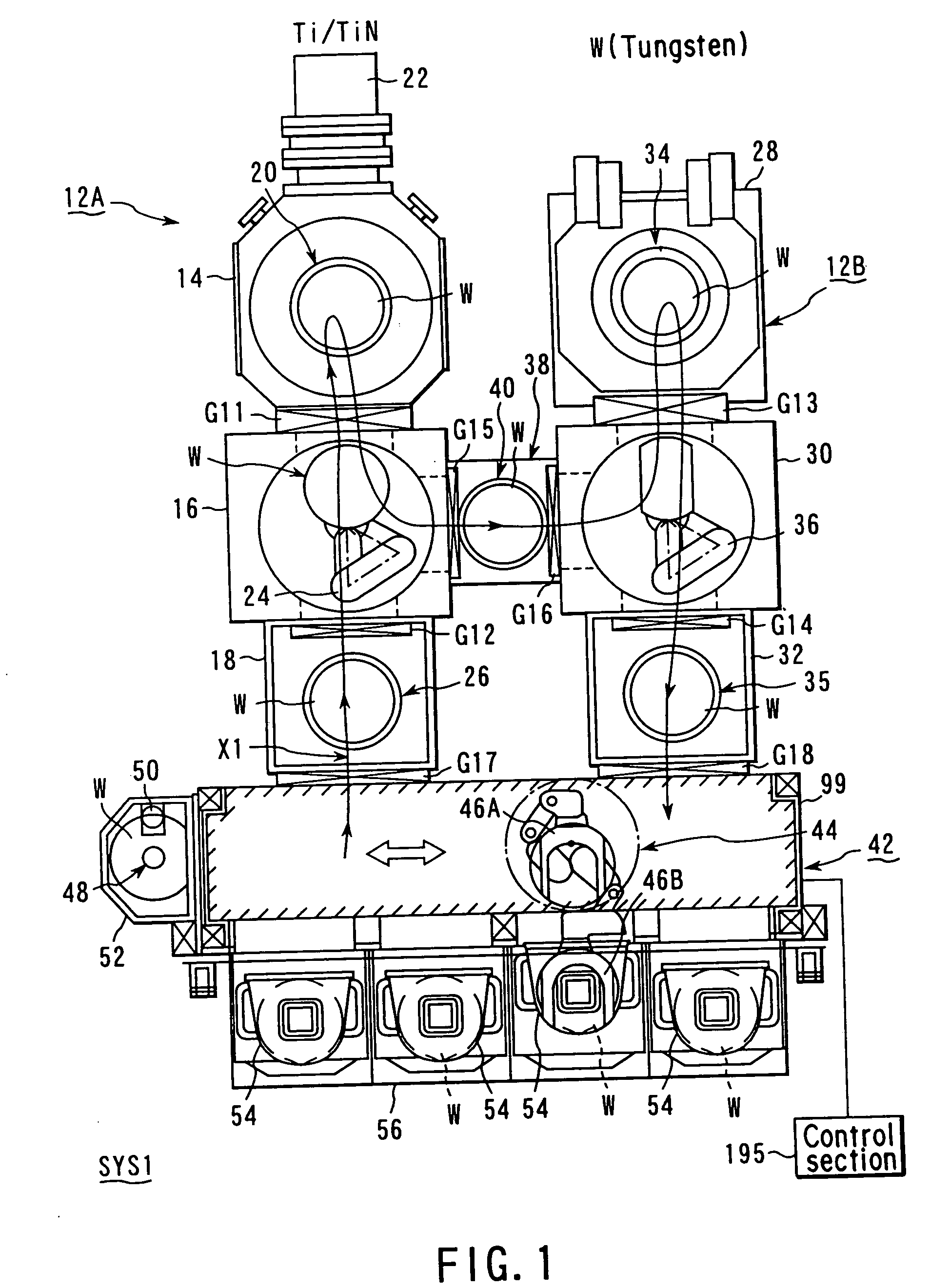
[0031] FIG. 1 is a schematic view showing the structure of a vacuum process system according to the present invention.
[0032] As is shown in the Figure, the vacuum process system SYS1 is mainly composed of a first process unit 12A for applying a first process to a semiconductor wafer W, or an object to be processed, and a second process unit 12B for applying a second process thereto.
[0033] Assume that a Ti / TiN film, for instance, is formed by sputtering in the first process unit 12A, and a tungsten film is formed by means of thermal CVD (Chemical Vapor Deposition) in the second process unit 12B.
[0034] The first process unit 12A includes a sputter process chamber 14 for performing a successive process on the Ti / TiN film by means of sputtering; a first transfer chamber 16 for transferring the semiconductor wafer W into / from the process chamber 14; and a first load lock chamber 18 for transferring the wafer W into / from the transfer chamber 16. The sputter process chamber 14 can be suppl...
third embodiment
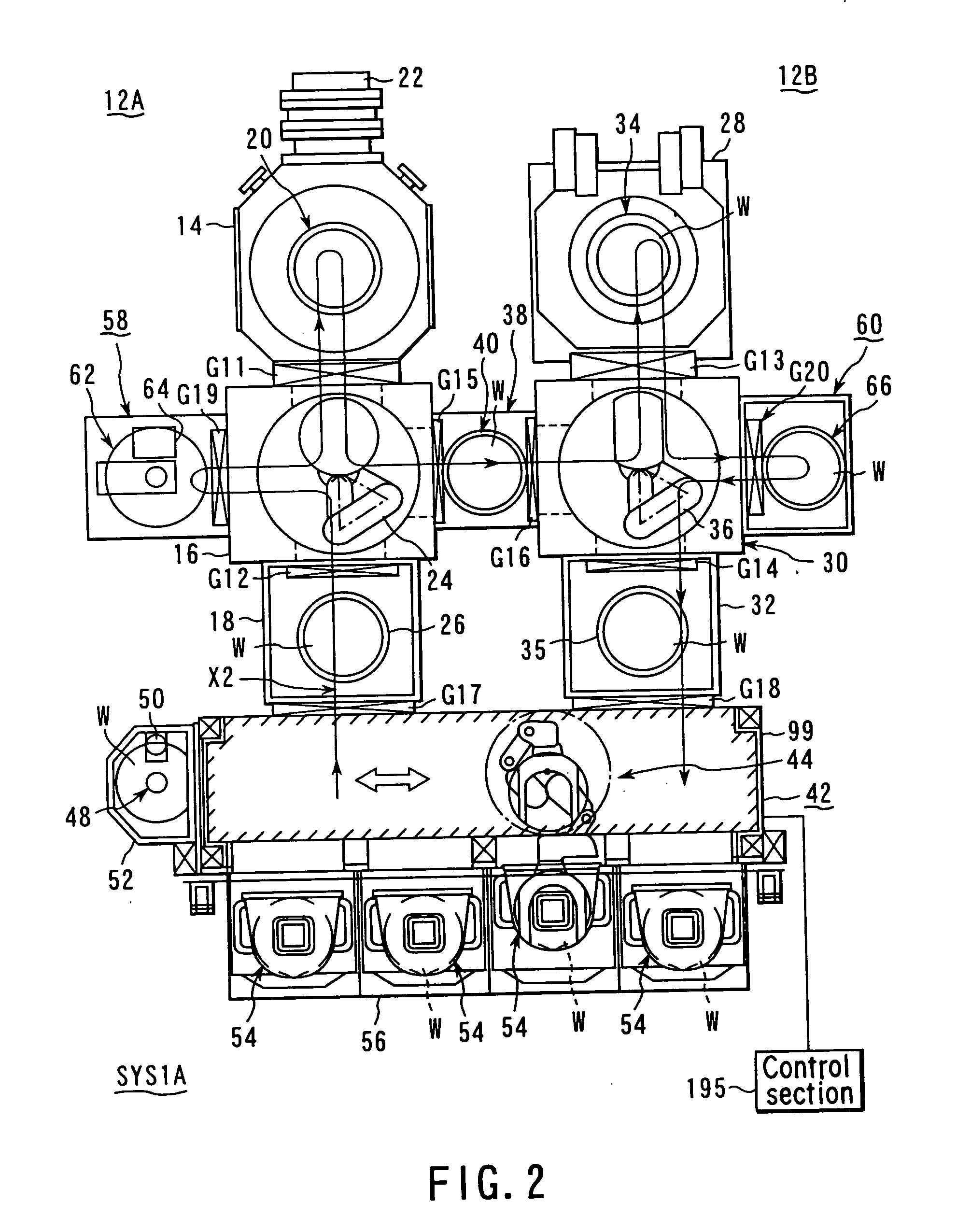
[0061] FIG. 3 shows the present invention. In a vacuum process system SYS1A' of this embodiment, the rotary table 62, which is rotatable and equipped with the heater, and the optical sensor 64 are provided in the first transfer chamber 16, whereby the wafer W is preheated and aligned at the same time. Each process unit 12A, 12B constitutes one module. Specifically, the process chamber 14, transfer chamber 16 and load lock chamber 18 are integrated to form one module. On the other hand, the process chamber 28, transfer chamber 30 and load lock chamber 32 are integrated to form one module. Each process unit (module) 12A, 12B is detachably attached to the process-object transfer stage 42 via a coupling section 119.
[0062] According to this embodiment, the wafer W is processed along substantially the same transfer path X2' as in the first embodiment, and thus the same operational advantage as in the first embodiment can be obtained. When maintenance for the process unit 12A (12B) is to b...
fifth embodiment
[0095] FIG. 11 shows the present invention. This embodiment is a modification of the structure shown in FIGS. 7 and 8. The structural parts common to those in FIGS. 7 and 8 are denoted by like reference numerals and a description thereof is omitted.
[0096] In this embodiment, two modules 204a and 204b, each comprising the vacuum process chamber 201 and the vacuum transfer chamber 203 including the transfer arm 202, are detachably attached to the transfer chamber 205 in a juxtaposed fashion.
[0097] As has been described above, in this embodiment, each module 204a, 204b comprises the process chamber 201 and the associated vacuum transfer chamber 203 and is individually connected to the common transfer chamber 205. In other words, the plural process-completion type modules 204a, 204b, in each of which the process chamber and vacuum transfer chamber are provided in a 1-to-1 relationship, are individually connected to the common transfer chamber 205. Accordingly, the flow of gas between th...
PUM
 Abstract
Description
Claims
Application Information
 - Generate Ideas
- Intellectual Property
- Life Sciences
- Materials
- Tech Scout
- Unparalleled Data Quality
- Higher Quality Content
- 60% Fewer Hallucinations
Browse by: Latest US Patents, China's latest patents, Technical Efficacy Thesaurus, Application Domain, Technology Topic, Popular Technical Reports.
© 2025 PatSnap. All rights reserved.Legal|Privacy policy|Modern Slavery Act Transparency Statement|Sitemap|About US| Contact US: help@patsnap.com