

Hydrogen assisted hdp-cvd deposition process for aggressive gap-fill technology
a technology of cvd film and hdp, which is applied in the field of manufacturing integrated circuits, can solve the problems of limiting the aspect ratio of gaps that hdp-cvd films are able to fill, affecting the efficiency of cvd film deposition, and affecting the ability to fill gaps. the effect of improving the gap-fill capability
- Summary
- Abstract
- Description
- Claims
- Application Information
AI Technical Summary
Benefits of technology
Problems solved by technology
Method used
Image

Examples
Embodiment Construction
Background of Invention
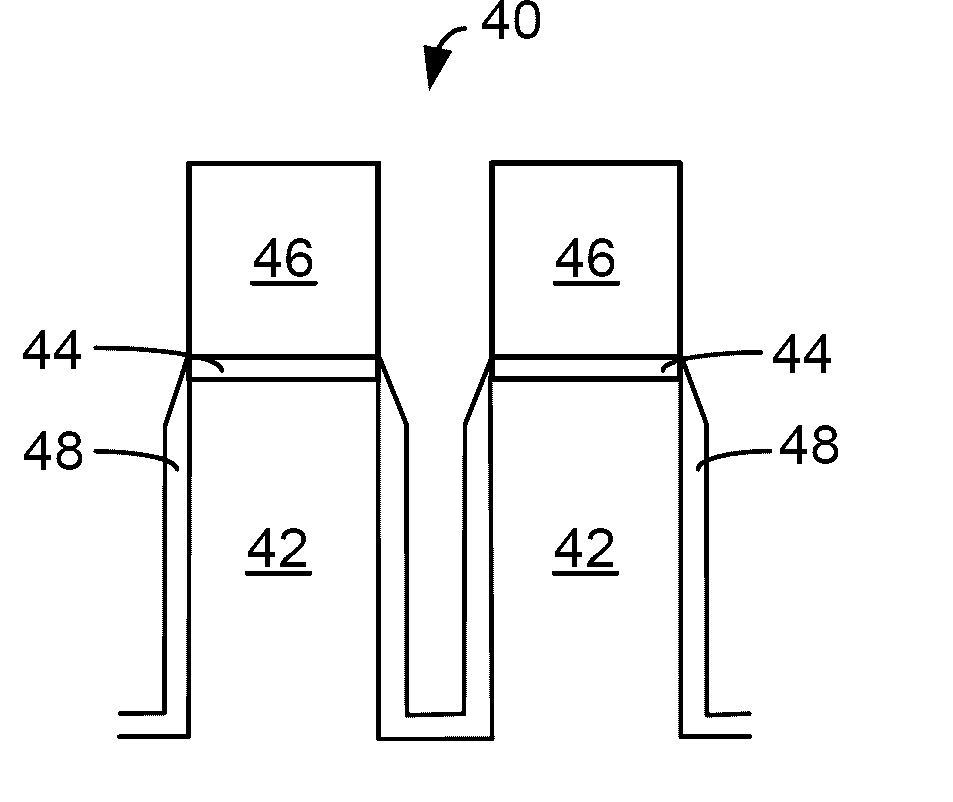
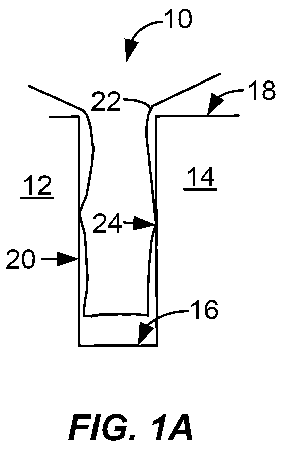
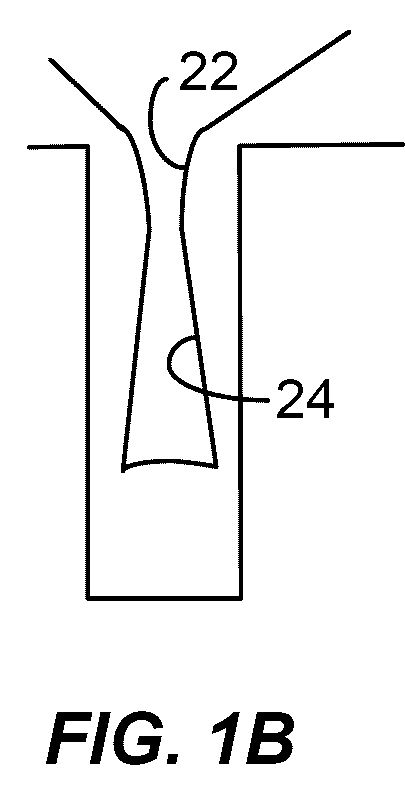
[0001] The present invention relates to the manufacture of integrated circuits. More specifically, the invention relates to an improved method of depositing silicon oxide layers for use as a dielectric material in such integrated circuits.
[0002] One of the primary steps in the fabrication of modern semiconductor devices is the formation of a film, such as a silicon oxide, on a semiconductor substrate. Silicon oxide is widely used as an insulating layer in the manufacture of semiconductor devices. As is well known, a silicon oxide film can be deposited by thermal chemical vapor deposition (CVD) or a plasma-enhanced chemical vapor deposition (PECVD) processes. In a conventional thermal CVD process, reactive gases are supplied to the substrate surface where heatchemical reactions (homogeneous or heterogeneous) take place to produce a desired film. In a conventional plasma process, a controlled plasma is formed to decompose and / or energize reactive species to prod...
PUM
| Property | Measurement | Unit |
|---|---|---|
| Fraction | aaaaa | aaaaa |
| Fraction | aaaaa | aaaaa |
| Flow rate | aaaaa | aaaaa |
Abstract
Description
Claims
Application Information