

Film carrier tape for mounting electronic devices thereon and production method thereof
- Summary
- Abstract
- Description
- Claims
- Application Information
AI Technical Summary
Benefits of technology
Problems solved by technology
Method used
Image

Examples
examples 1 to 3
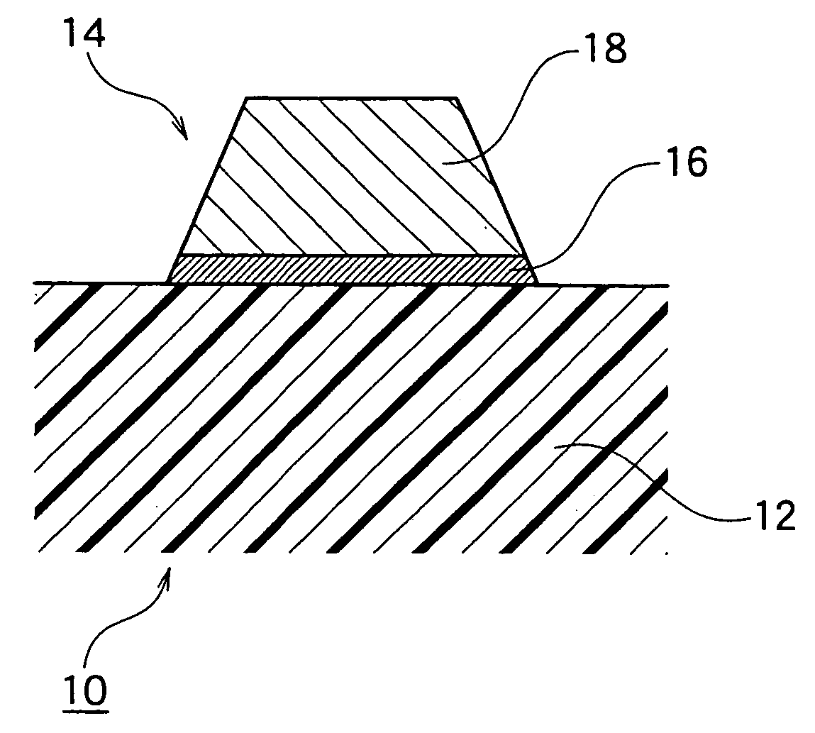
[0117] Surface of 125 .mu.m thick polyimide film (trade name: Kapton, produced by Du Pont Toray Co., Ltd.)) was treated by inverse sputtering. The treated surface was coated with elemental zinc by sputtering, thereby forming a zinc layer of 100 angstroms thickness in Example 1 and a zinc layer of 200 angstroms thickness in Example 2. Subsequently, the surface of the zinc layer was coated with nickel by sputtering, thereby forming a nickel layer of 300 angstroms thickness. Thereafter, the surface of the nickel layer was coated with copper by sputtering, thereby forming a copper layer of 5000 angstroms thickness. After the formation of seed layer in the above manner, electroplating was carried out in a copper sulfate plating bath, thereby forming an 8 .mu.m thick electrodeposited copper foil layer on the surface of the seed layer. Thus, a double layer flexible substrate was obtained.
[0118] In Example 3, a surface of 125 .mu.m thick polyimide film (trade name: Kapton, produced by Du Po...
example 4
[0120] Surface of 125 .mu.m thick polyimide film (trade name: Kapton, produced by Du Pont Toray Co., Ltd.)) was treated by inverse sputtering. The treated surface was coated with an alloy consisting of 10 mass % of elemental zinc, 80 mass % of elemental nickel and 10 mass % of elemental copper by sputtering, thereby forming an alloy layer of 150 angstroms thickness. After the formation of seed layer in the above manner, electroplating was carried out in a copper sulfate plating bath, thereby forming an 8.mu.m thick electrodeposited copper foil layer on the surface of the seed layer. Thus, a double layer flexible substrate was obtained.
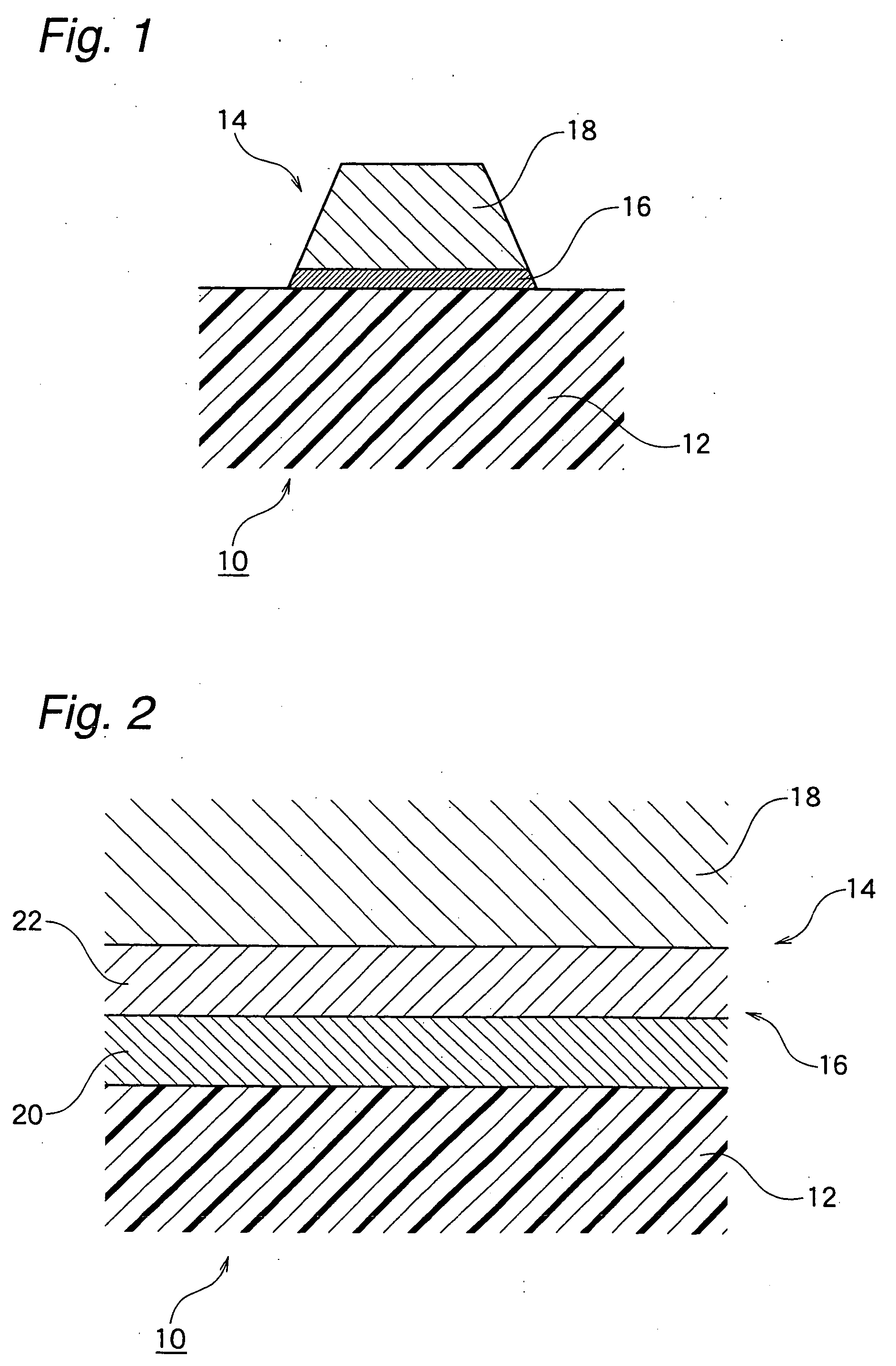
[0121] The thus obtained double layer flexible substrate was slit into a 35 mm width long tape. The surface of electrodeposited copper foil layer thereof was coated with photoresist (trade name: FR-200, produced by Shipley Far East Ltd.), dried, exposed to UV through a glass photomask provided with a 50 .mu.m pitch comb-shaped electrode pattern of conf...
example 5
[0127] Surface of 125 .mu.m thick polyimide film (trade name: Kapton, produced by Du Pont Toray Co., Ltd.)) was treated with plasma. The treated surface was coated with a nickel-chromium alloy by sputtering, thereby forming a seed layer of 65 angstroms thickness. Thereafter, electroplating was carried out in a copper sulfate plating bath, thereby forming an 8.mu.m thick electrodeposited copper foil layer on the surface of the seed layer. Thus, a double layer flexible substrate was obtained.
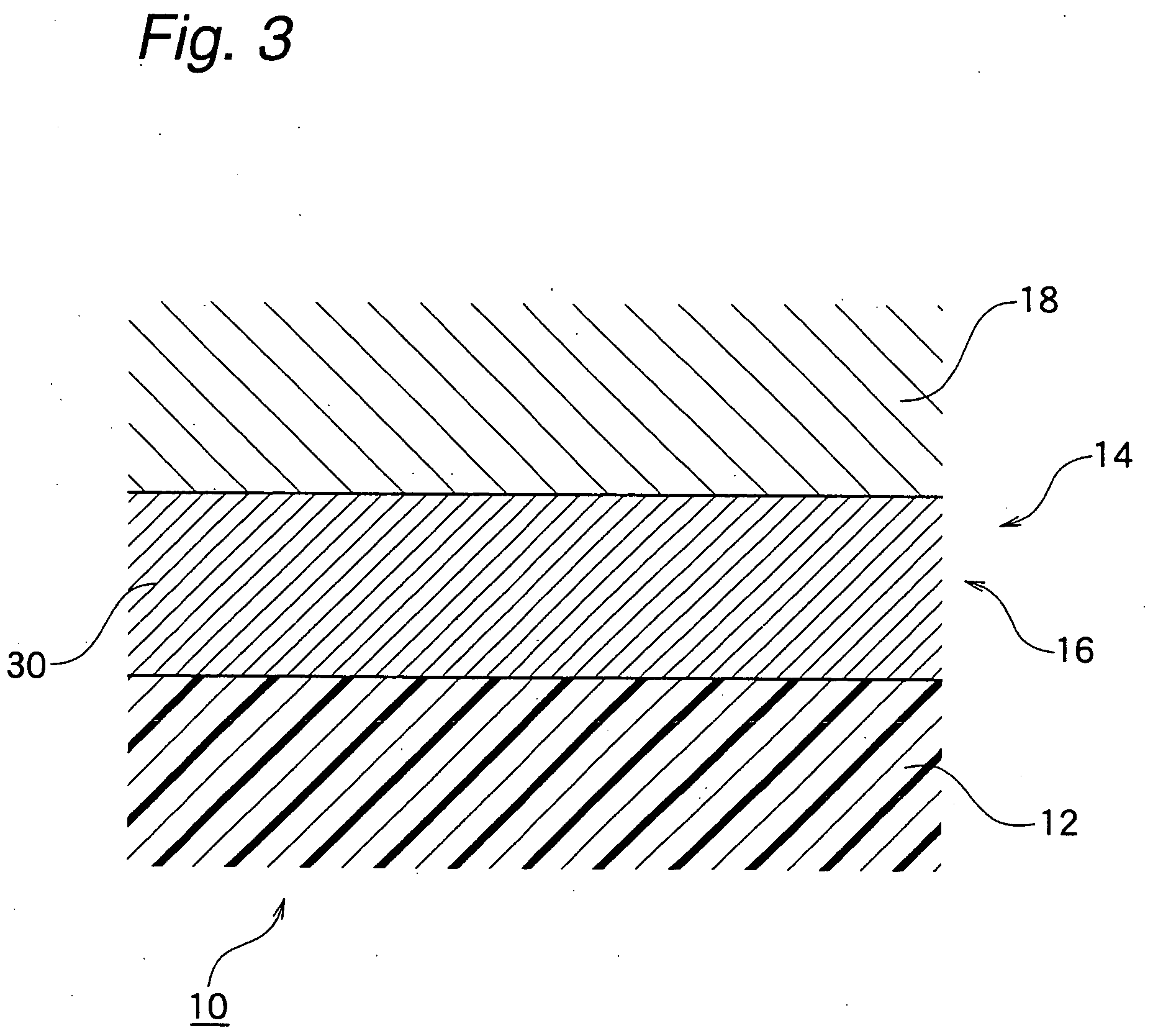
[0128] The thus obtained double layer flexible substrate was slit into a 35 mm width long tape. According to customary procedure, the surface of electrodeposited copper foil layer thereof was coated with photoresist (trade name: FR-200, produced by Shipley Far East Ltd.), dried, exposed to UV through a glass photomask provided with a 50 .mu.m pitch comb-shaped electrode pattern-of configuration shown in FIG. 6, and developed with alkali (KOH). Thereafter, etching thereof was carried out at 40.degr...
PUM
| Property | Measurement | Unit |
|---|---|---|
| Percent by mass | aaaaa | aaaaa |
| Percent by mass | aaaaa | aaaaa |
| Percent by mass | aaaaa | aaaaa |
Abstract
Description
Claims
Application Information