Method for fabricating a contact hole plane in a memory module

a memory module and contact hole technology, applied in the field of memory module contact hole plane fabrication, can solve the problems of gate electrode track attack and damage, the process that is to be performed in the contact opening becomes increasingly difficult, and the electrical properties of the memory cells are at risk, so as to achieve high selectivity, high etching resistance, and high precision of material plug structur

Inactive Publication Date: 2005-01-06
POLARIS INNOVATIONS LTD
View PDF6 Cites 29 Cited by
  • Summary
  • Abstract
  • Description
  • Claims
  • Application Information

AI Technical Summary

Benefits of technology

[0010] According to one aspect of the invention, an optimized process implementation is provided for fabricating bit line contacts in a memory module. This process implementation is distinguished by a low coupling capacitance between bit line contacts and gate electrode tracks and enabling a reliable and damage-free bit line contact fabrication in a simple manner.

Problems solved by technology

This gap narrowing increases the aspect ratio, that is to say, the ratio of width to height of the contact openings, as a result of which processes that are to be performed in the contact openings become increasingly more difficult.
This problem is intensified from DRAM generation to DRAM generation on account of the ever smaller lateral dimensions.
Furthermore, owing to its high dielectric constant, the silicon nitride spacer in the contact hole leads to a strong coupling between the conductive material in the bit line contact and the gate electrode tracks, so that there is the risk of the electrical properties of the memory cells being impaired.
The use of silicon nitride as a spacer for forming the bit line contacts has the disadvantage, moreover, that, on account of the directional etching required, an etching process with a high sputtering element is required, it being possible for the gate electrode tracks to be attacked and damaged particularly in the upper edge region.

Method used


Image

  • Method for fabricating a contact hole plane in a memory module
  • Method for fabricating a contact hole plane in a memory module
  • Method for fabricating a contact hole plane in a memory module

Examples


Embodiment Construction

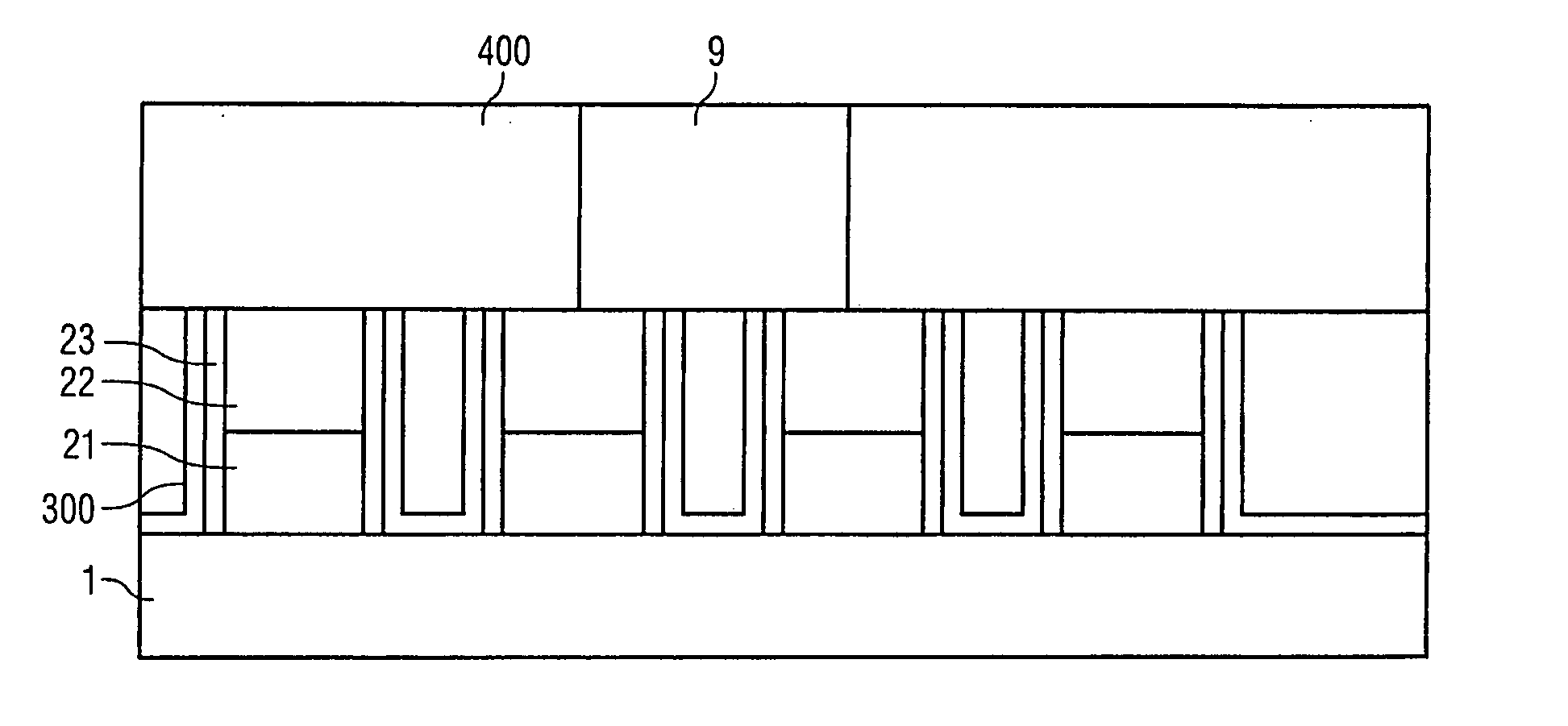
[0029] The invention is illustrated by way of example using a process sequence for fabricating a contact hole plane in a DRAM module with a memory cell region and a logic region on a silicon wafer. However the invention can be used to form any desired contacts between gate electrode tracks in semiconductor modules.

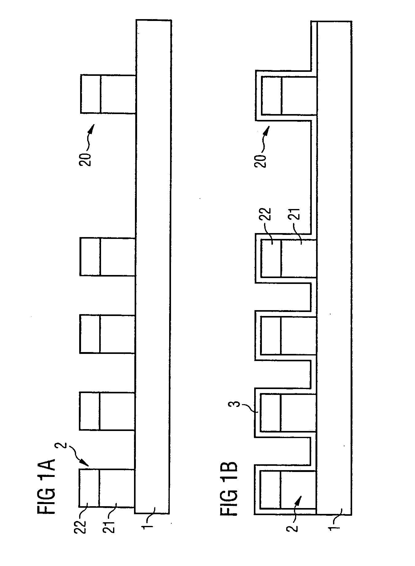
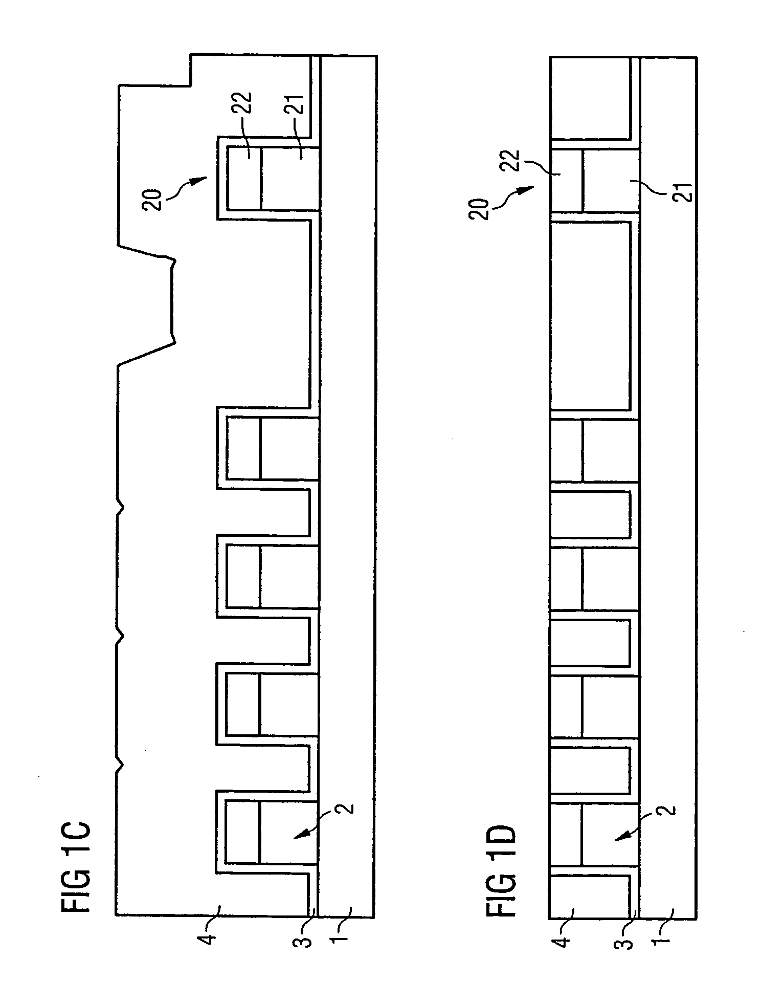
[0030]FIGS. 1A to 1O respectively show a cross section through a detail from a prepatterned silicon wafer 1, on which a memory cell region and a peripheral logic region are provided. In this case, the memory cells of the DRAM are composed of a selection transistor and a storage capacitor. The peripheral logic region contains various components for driving the memory cells.

[0031]FIG. 1A shows the starting point, the prepatterned silicon wafer 1 (structures are not shown), on which are formed a cell array, represented by four gate electrode tracks 2 spaced apart equidistantly, and a logic region separate therefrom, represented by a further gate electrode track 20. In parti...


PUM

PropertyMeasurementUnit
thicknessaaaaaaaaaa
thicknessaaaaaaaaaa
thicknessaaaaaaaaaa

Abstract

In order to fabricate a contact hole plane in a memory module with an arrangement of memory cells each having a selection transistor, on a semiconductor substrate with an arrangement of mutually adjacent gate electrode tracks on the semiconductor surface, an insulator layer is formed on the semiconductor surface and a sacrificial layer is subsequently formed on the insulator layer, then material plugs are produced on the sacrificial layer for the purpose of defining contact openings between the mutually adjacent gate electrode tracks, the sacrificial layer is etched to form material plugs with the underlying sacrificial layer blocks, after the production of the vitreous layer with uncovering of the sacrificial layer blocks above the contact openings between the mutually adjacent gate electrode tracks, an essentially planar surface being formed, then the sacrificial layer material is etched out from the vitreous layer and the uncovered insulator material is removed above the contact openings on the semiconductor surface and, finally, the contact opening regions are filled with a conductive material.

Description

CLAIM FOR PRIORITY [0001] This application claims priority to German application No. 103 14 274.6 filed Mar. 29, 2003. TECHNICAL FIELD OF THE INVENTION [0002] The invention relates to a method for fabricating a contact hole plane in a memory module with an arrangement of memory cells each having a selection transistor and in particular to a dynamic random access memory (DRAM). BACKGROUND OF THE INVENTION [0003] DRAMs are composed of a multiplicity of memory cells which are formed regularly in the form of a matrix on a semiconductor wafer. Said memory cells generally comprise a storage capacitor and a selection transistor. During a read or write operation, the storage capacitor is charged or discharged, via the selection transistor, with an electrical charge corresponding to the respective data unit (Bit). For this purpose, the selection transistor is addressed with the aid of a bit line and a word line. [0004] DRAMs are generally realized with the aid of planar technology. The latte...

Claims


Application Information

Patent Timeline
Patent Type & Authority Applications(United States)
IPC IPC(8): H01L21/60H01L21/768H01L21/8242
CPCH01L21/76828H01L21/76829H01L21/76832H01L27/10894H01L21/76837H01L21/76897H01L27/10888H01L21/76834H10B12/485H10B12/09
Inventor FROHLICH, HANS-GEORGGENZ, OLIVERGRAF, WERNERGRUSS, STEFANHANDKE, MATTHIASHEGER, PERCYHEINECK, LARSLAESSIG, ANTJEREB, ALEXANDERSCHUPKE, KRISTINSTAVREV, MOMTCHILVOGT, MIRKO
Owner POLARIS INNOVATIONS LTD
Why Eureka
Try Eureka