

Integrated stacked capacitor and method of fabricating same
a technology of integrated stacked capacitors and capacitors, which is applied in the direction of capacitors, semiconductor devices, electrical equipment, etc., can solve the problems of high leakage current rate of materials, difficult to meet the demand for ever-smaller chip sizes, and high difficulty in component fabrication, so as to achieve flexible application and enhance performance.
- Summary
- Abstract
- Description
- Claims
- Application Information
AI Technical Summary
Benefits of technology
Problems solved by technology
Method used
Image

Examples
Embodiment Construction
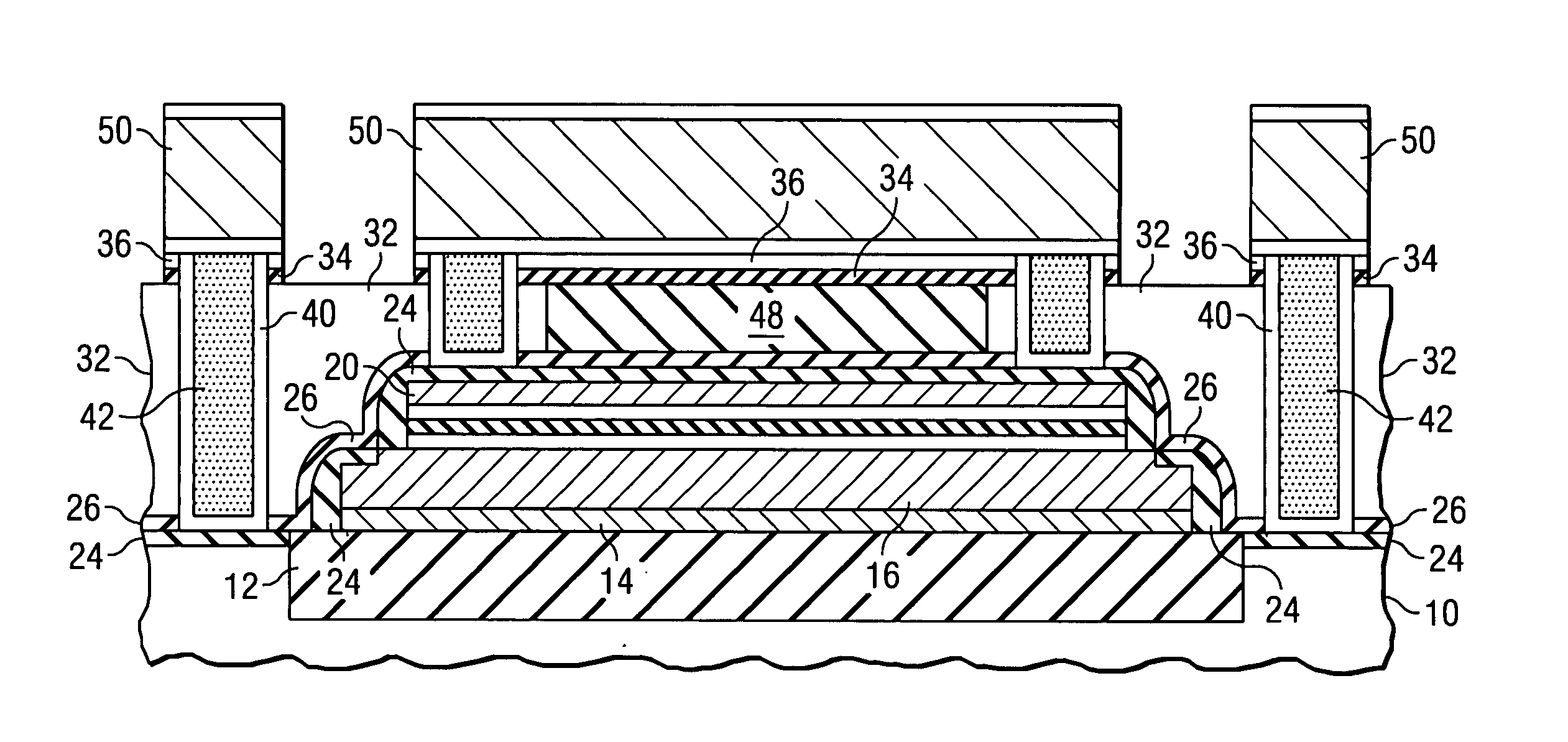
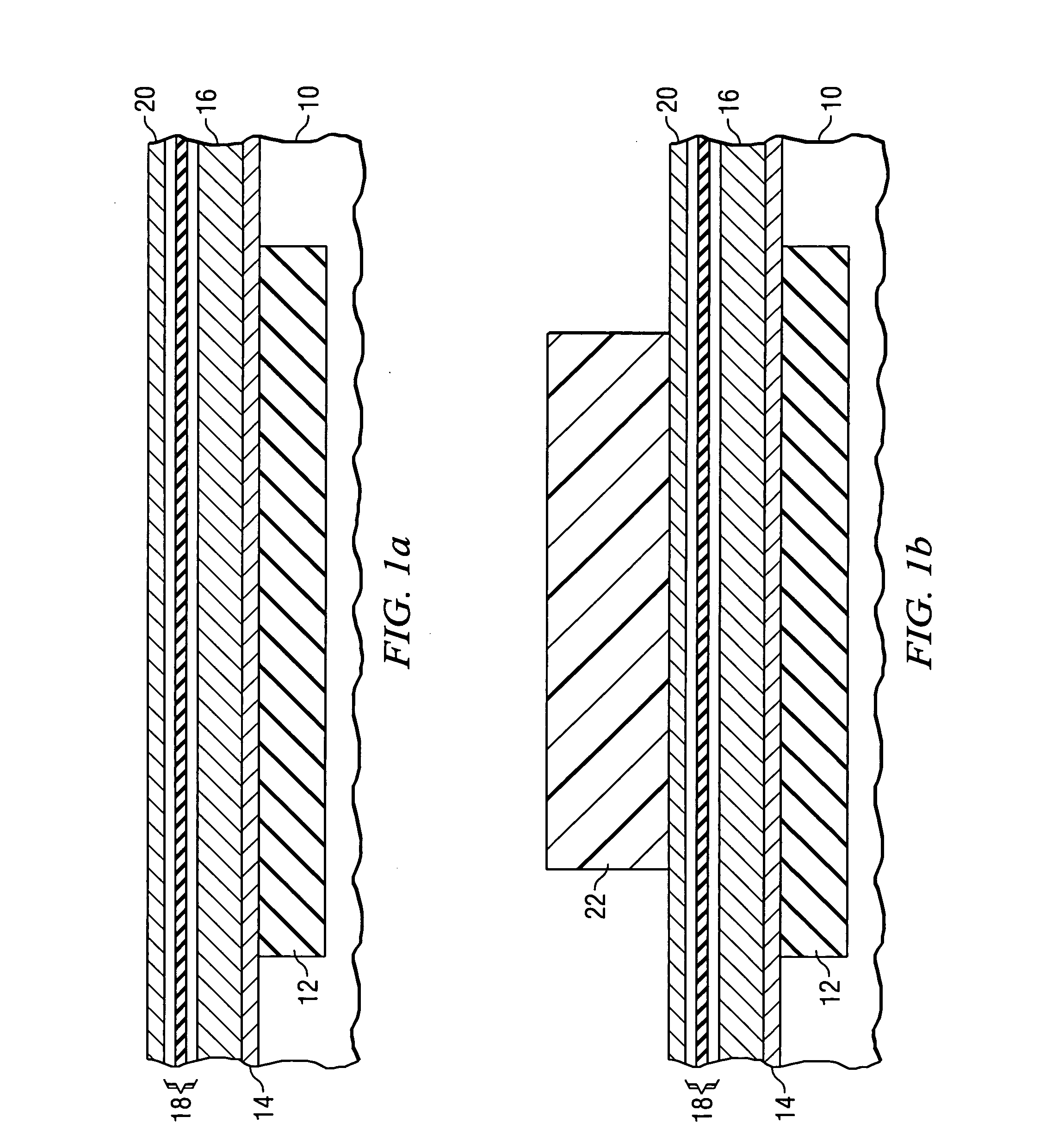
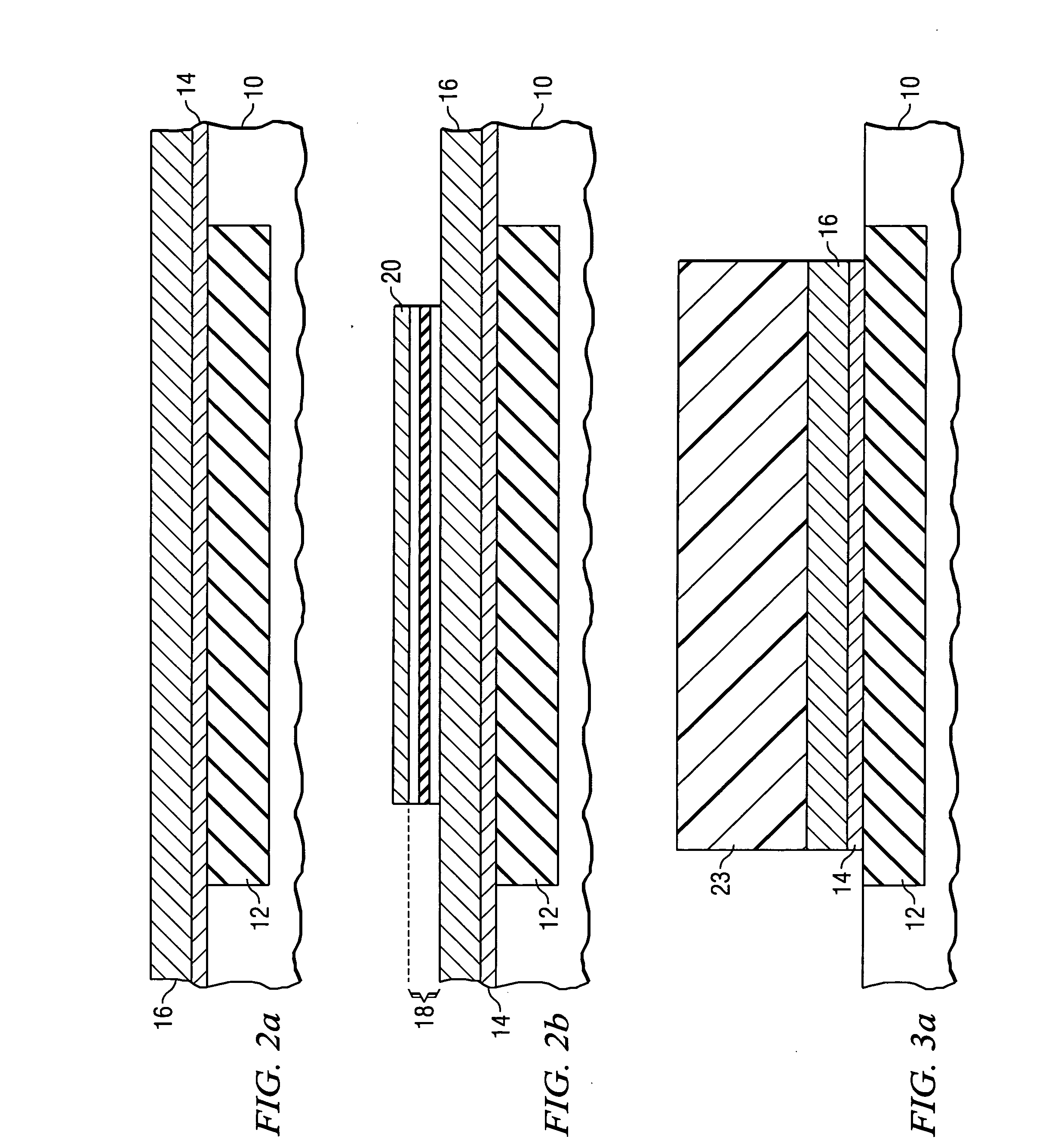
[0019] For a capacitor according to the invention, a second dielectric and a third capacitor film are provided, the second dielectric being sandwiched between the second capacitor film and the third capacitor film. The invention thus provides a MIMIM (metal-insulator-metal-insulator-metal) parallel plate capacitor in which the second capacitor film is not a cover plate but a middle film sandwiched between two outer capacitor films, with a dielectric being provided between the films in each case. The capacitor according to the invention is distinguished by a high capacitive density and is compatible with a variety of applications by suitably circuiting the individual capacitor films.
[0020] The second (middle) film preferably consists of titanium nitride or a titanium alloy.
[0021] For certain applications it is of advantage when the first dielectric consists of a nitride and the second dielectric of an oxide or when the first dielectric and second dielectric each consist of a nitrid...
PUM
 Abstract
Description
Claims
Application Information