DRAM memory circuit with sense amplifiers

a memory circuit and amplifier technology, applied in the direction of amplifiers with semiconductor devices/discharge tubes, dc-amplifiers with dc-coupled stages, instruments, etc., can solve the problems of increasing the area requirement of the integrated circuit, becoming ever more difficult to control, and extremely undesirable amplifier behavior, etc., to achieve fewer doping steps

Inactive Publication Date: 2005-01-13
POLARIS INNOVATIONS LTD
View PDF3 Cites 9 Cited by
  • Summary
  • Abstract
  • Description
  • Claims
  • Application Information

AI Technical Summary

Benefits of technology

[0017] The use of field-effect transistors of a single conduction type also has the advantage that fewer doping steps are necessary during production.

Problems solved by technology

The doping profile at the boundary between a P-type well that is to be formed for the N-FETs and an N-type well that is to be formed for the P-FETs thus becomes ever more difficult to control with increasing miniaturization of the feature sizes.
In a sense amplifier, a one-sided alteration of the threshold voltage may lead to an extremely undesirable asymmetry of the amplifier behavior.
This safety zone is in principle an unused space and thus undesirably increases the area requirement of the integrated circuit.
The smaller the safety zones are made in order to reduce the area requirement, the greater the risk of the aforementioned asymmetry and, consequently, rejects in chip production.

Method used


Image

  • DRAM memory circuit with sense amplifiers
  • DRAM memory circuit with sense amplifiers
  • DRAM memory circuit with sense amplifiers

Examples


Embodiment Construction

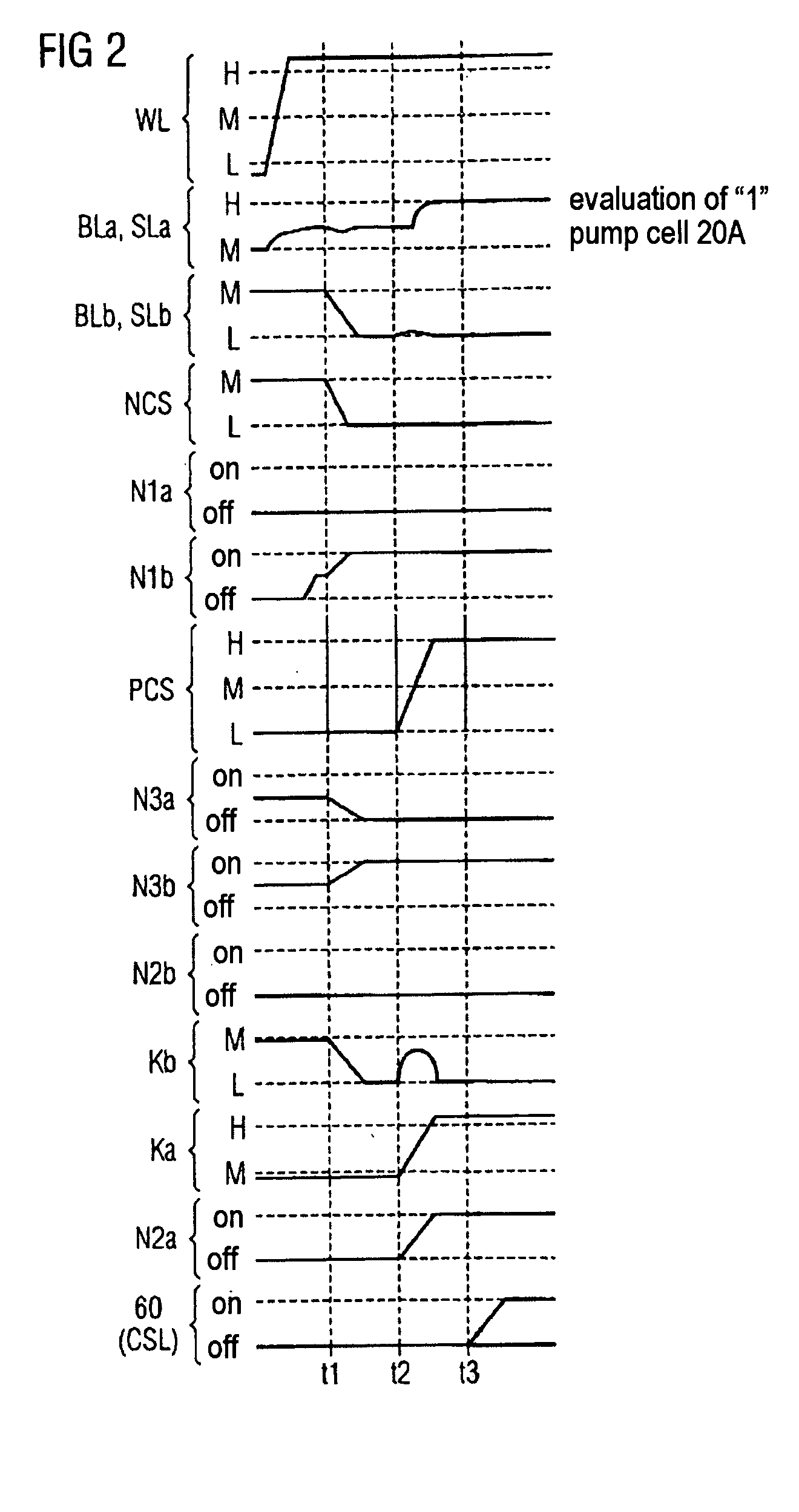
[0021] For the description below and the drawings, the following notation shall apply with regard to the electrical potentials: the two logic potentials are designated by “L” for “low” and by “H” for “high”. In the example described, H is positive with respect to L; the comparative “higher” thus means “more positive” and the comparative “lower” means “less positive” or “more negative”.

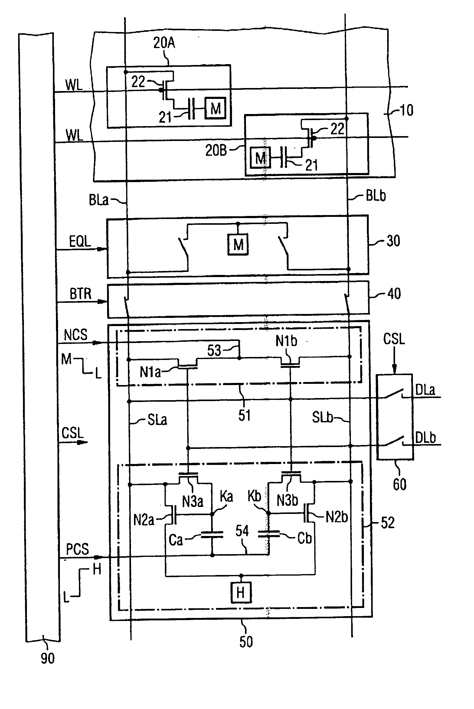
[0022] In its upper part, FIG. 1 shows a detail from the edge region of a cell array 10 of a DRAM memory circuit. A large number of cell arrays, combined in one or more “banks”, are usually integrated on a memory chip. The illustration shows the last two memory cells 20A and 20B of a column of the cell array 10 and the bit line cores BLa and BLb associated with said column. Each memory cell contains a storage capacitance (capacitor) 21, which forms the actual memory element in which a binary datum can be stored as an electrical charge. One side of the capacitor 21 is connected to a fixed potential, pr...


PUM


Abstract

In a DRAM memory circuit, the sense amplifiers, for amplifying the differential voltage sensed between the cores of a bit line, in each case contain two transistor circuits, each of which has two switching transistors. The first transistor circuit pulls the lower potential of the sensed differential voltage down to a defined low logic potential. The second transistor circuit pulls the higher potential up to a defined high logic potential. According to the invention, all the transistors in the sense amplifier are field-effect transistors of the same conduction type, in the case of which the channel is at low impedance if the gate potential is higher than the source potential at least by the amount of the threshold voltage Vth. The second transistor circuit may contain, for each of its two switching transistors, in each case a pump circuit in order to boost the gate of that switching transistor which is intended to pull up the higher logic potential to a potential which is higher than the high logic potential by at least the amount of the threshold voltage Vth.

Description

CROSS-REFERENCE TO RELATED APPLICATIONS [0001] This application claims foreign priority benefits under 35 U.S.C. §119 to co-pending German patent application number 103 22 544.7-55, filed May 20, 2003. This related patent application is herein incorporated by reference in its entirety. BACKGROUND OF THE INVENTION [0002] 1. Field of the Invention [0003] The invention relates to a DRAM memory circuit with sense amplifiers. As is known, the acronym DRAM stands for digital random access memory having a multiplicity of memory cells which are directly selectively addressable in order optionally to write in or read out binary memory data at said memory cells. [0004] 2. Description of the Related Art [0005] DRAMs usually contain one or more cell arrays, each of which contains a multiplicity of memory cells forming a matrix-type arrangement of rows and columns. Each column is assigned a column line, which comprises two cores and is referred to as a “bit line”. Each row is assigned a row sele...

Claims


Application Information

Patent Timeline
Patent Type & Authority Applications(United States)
IPC IPC(8): G11C7/06G11C11/4091
CPCG11C11/4091G11C7/06
Inventor SOMMER, MICHAEL
Owner POLARIS INNOVATIONS LTD
Why Eureka
Try Eureka