Organic light emitting diode (oled)

a light-emitting diode and organic technology, applied in the direction of discharge tube/lamp details, discharge tube luminescnet screens, other domestic objects, etc., can solve the problems of reducing the electron injection efficiency of the device, cathode defects such as pinholes, and limited life of such devices

Inactive Publication Date: 2005-01-20
AGENCY FOR SCI TECH & RES +1
View PDF14 Cites 25 Cited by
  • Summary
  • Abstract
  • Description
  • Claims
  • Application Information

AI Technical Summary

Benefits of technology

[0048] This dielectric layer preferably has a thickness which is within electron tunneling range. This dielectric layer is adapted to lower the effective barrier height for electron injection and thereby enhance the luminescence quantum efficiency of the OLED.
[0112] When a barrier layer is formed on the EL layer, the cathode may be deposited by sputtering as the barrier layer will protect the EL layer from ion bombardment.

Problems solved by technology

Although remarkably stable electroluminescent (EL) devices have been demonstrated operating in inert environments, the lifetimes of such devices have been limited by the formation and growth of non-emissive areas known as “dark spots.”
One such factor is cathode defects such as pinholes.
The oxidized cathode reduces the electron injection efficiency of the device and a higher driving bias is therefore needed.
This significantly increases the chance of local shorting.
Although sputtering is one of the methods commonly used in the semiconductor industry for the deposition of cathodes, this technique has, until now, not been suitable for OLEDs.
This is because OLEDs are extremely sensitive and are damaged by the radiation, charging, heating and ion bombardment involved in the sputtering process.
Although sputtering produces cathodes with few or no pinholes, it has not been used on OLEDs because of the damage caused by the technique.
The diffusion of moisture and oxygen through the layers of the OLED is a significant cause of the growth of dark spots on the cathode.
Magnesium and Calcium are often used as cathode materials in OLED devices because of their low work function.
However, Calcium and Magnesium are very sensitive to oxygen and water vapor.
This heating is often caused by high currents.
It expedites material failure, increases the possibility of inter-diffusion of the organic layers and leads to dark spot growth.
A further problem faced by prior art OLEDs is that they do not have very good polymer stability.
However, because these advanced OLEDs also exhibit dark spot formation and growth they therefore have a relatively short lifespan.

Method used


Image

  • Organic light emitting diode (oled)
  • Organic light emitting diode (oled)
  • Organic light emitting diode (oled)

Examples


Embodiment Construction

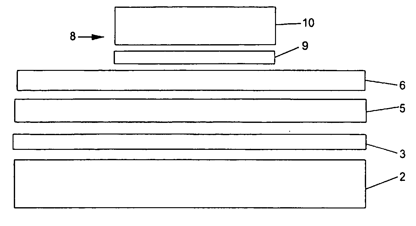
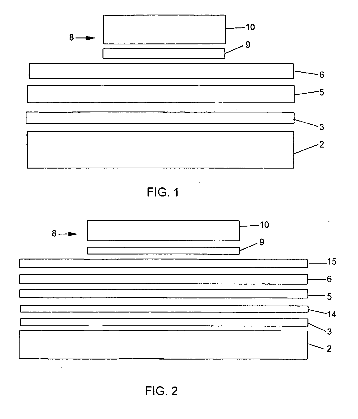
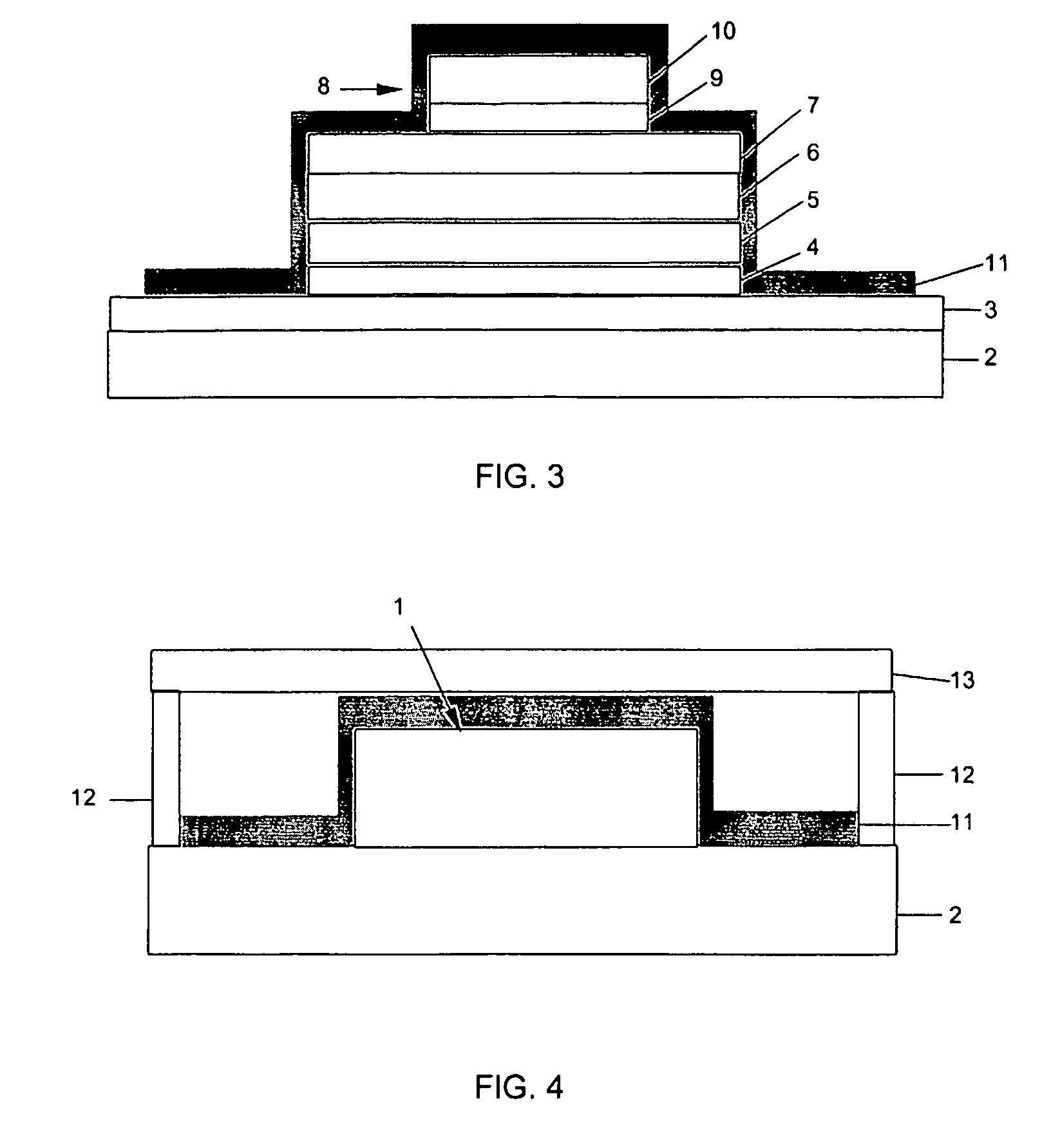
[0122] Referring to the drawings, FIG. 3 shows a schematic cross-sectional view of a first preferred embodiment of the OLED of the present invention. As seen in that Figure, the OLED 1 includes a number of layers disposed on a substrate 2. In this embodiment, the layers are arranged in the following order: an anode 3, a first oxygen / moisture barrier 4, a hole transport layer 5, and electroluminescent (EL) layer 6, a second oxygen / moisture barrier 7 and a cathode 8. In this embodiment the cathode 8 includes a calcium cathode layer 9 and a silver / aluminum cathode layer 10. All of these layers are at least partially encapsulated by an encapsulation layer 11.

[0123] The first oxygen / moisture barrier 4 is adapted to resist permeation by oxygen and moisture and is also designed to inhibit metal migration. In this preferred embodiment the barrier 4 is an organic barrier made from a polymer selected from polyimides, teflon and parylene. It is between 1 and 20 nm thick and is deposited on th...


PUM


Abstract

An Organic Light Emitting Diode (OLED) which is adapted to inhibit the formation and growth of non-emissive areas known as “dark spots.” The OLED comprises an anode disposed on a substrate, a cathode, an electroluminescent (EL) layer disposed between the anode and the cathode and a hole transport layer disposed between the anode and the EL layer. The OLED has one or more dielectric organic barrier layers disposed between one or more of the OLED's layers. These barrier layers are made from an organic polymer and are adapted to resist permeation by oxygen and moisture and to inhibit metal migration.

Description

TECHNICAL FIELD [0001] The present invention relates to Organic Light Emitting Diodes (OLEDs) and, in particular, to an OLED which is adapted to inhibit the formation and growth of non-emissive areas known as “dark spots.”[0002] The invention is particularly suitable for OLEDs used in flat panel displays, and will be described hereinafter with reference to this application. However, it will be appreciated that the invention is not limited to this particular field of use. BACKGROUND ART [0003] A typical OLED consists of two electrodes with one or more polymer layers disposed between the electrodes. As shown in FIG. 1, these devices commonly include the following layers, arranged in the following order: [0004] (i) a substrate 2 often made from plastic or glass; [0005] (ii) an anode 3 disposed on the substrate and commonly made from a transparent conductive material, which may be an organic material or an inorganic oxide such as Indium Tin Oxide (ITO); [0006] (iii) a hole transport lay...

Claims


Application Information

Patent Timeline
Patent Type & Authority Applications(United States)
IPC IPC(8): H01L51/50H05B33/22H01L51/52H05B33/04
CPCH01L51/5237H01L51/5221Y10S428/917H10K50/82H10K50/844
Inventor KE, LINRAMADAS, SENTHIL KUMARCHUA, SOO JIN
Owner AGENCY FOR SCI TECH & RES
Why Eureka
Try Eureka