Substrate holding device, substrate processing apparatus using the same, and method for aligning and holding substrate

a technology for holding devices and substrates, applied in photomechanical devices, instruments, printers, etc., can solve problems such as further separation of holding units

Inactive Publication Date: 2005-01-27
CANON KK
View PDF17 Cites 11 Cited by
  • Summary
  • Abstract
  • Description
  • Claims
  • Application Information

AI Technical Summary

Benefits of technology

[0007] According to the present invention, a substrate holding device includes a substrate holding unit and supporting elements protruding from a substrate-holding surface of the substrate holding unit. The substrate holding unit holds a substrate in a predetermined state by a first holding force after the relative positions of the substrate and the substrate holding unit are adjusted while the supporting elements lift the substrate off the substrate-holding surface, and the substrate holding unit holds the substrate by zero holding force or a second holding force that is smaller than the first holding force before the relative positions of the substrate and the substrate holding unit are adjusted. Thus, the substrate holding device can align the substrate in a short time and hold it.
[0008] Preferably, the substrate holding device moves the substrate holding unit to a point for measuring a positional deviation of the substrate, while the substrate holding unit is holding the substrate by zero holding force or a second holding force, before the relative positions of the substrate and the substrate holding unit are adjusted. Thus, the substrate holding device can align the substrate with a reference coordinate in a short time.
[0009] Preferably, the substrate holding device moves the substrate holding unit to correct a positional deviation of the substrate from a reference coordinate and to align the substrate with the substrate holding unit. More preferably, the positional deviation is a deviation in the rotational direction. In this case, since a maximum rotation stroke is limited, adjustment of the positions of the substrate and the substrate holding unit is further required. Accordingly, the throughput is efficiently increased.
[0011] In recent years, the wavelength of exposure light has been decreased in order to achieve exposure systems with high resolution. These shortened wavelengths require exposure in a vacuum atmosphere as an exposure environment. In a vacuum atmosphere, however, a wafer must be held with electrostatic attraction instead of vacuum attraction. Electrostatic attraction requires a considerable amount of time to release the wafer, thus decreasing the throughput. Accordingly, when the wafer is held with electrostatic attraction, the above-described structure can improve the throughput more efficiently.
[0013] According to another aspect of the present invention, a method for aligning a substrate with a reference position in a substrate processing apparatus includes the steps of mounting the substrate on a holding surface; holding the substrate on the holding surface by a second holding force smaller than a first holding force, which is used for holding the substrate during processing of the substrate; measuring a positional deviation of the substrate from the reference position; moving the substrate to correct the deviation while holding the substrate by the second holding force; lifting the substrate off the holding surface; moving the holding surface relative to the substrate; and transferring the substrate to the holding surface. Thus, the substrate processing apparatus can align the substrate in a short time and hold it.

Problems solved by technology

In this case, since a maximum rotation stroke is limited, adjustment of the positions of the substrate and the substrate holding unit is further required.

Method used


Image

  • Substrate holding device, substrate processing apparatus using the same, and method for aligning and holding substrate
  • Substrate holding device, substrate processing apparatus using the same, and method for aligning and holding substrate
  • Substrate holding device, substrate processing apparatus using the same, and method for aligning and holding substrate

Examples


first embodiment

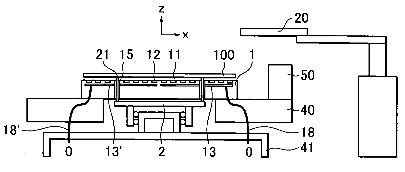
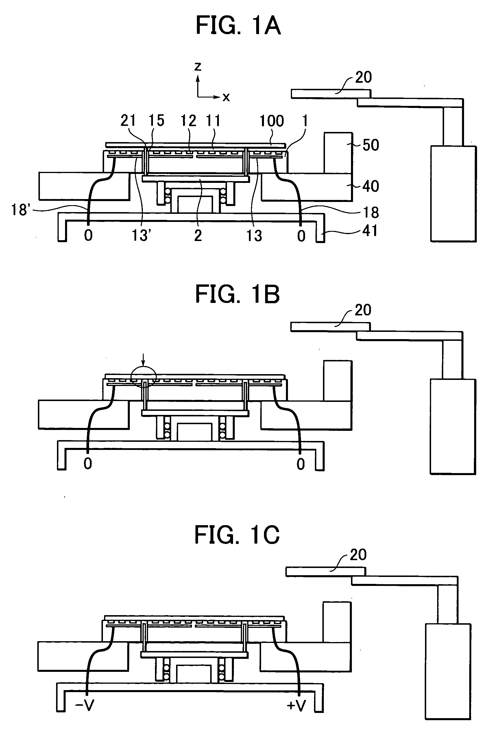
[0023]FIG. 1 shows a first embodiment of the present invention. A substrate holding device is included in an exposure system. The Z-axis is the direction of the optical axis of exposure light. The substrate holding device includes a top plate supporting table 41 mounted on a translation stage 60, shown in FIG. 5, which has a long stroke movement in the X and Y directions perpendicular to the Z-axis direction; a top plate 40 having short stroke movements in the Z direction and about the Z-axis with respect to the top plate supporting table 41; and a chuck 1 which is secured on the top plate 40 and serves as substrate holding means to hold a substrate or wafer 100. The top plate 40 includes a measurement mirror 50 for an interferometer 160, shown in FIG. 5, which is used to measure the position of the top plate 40.

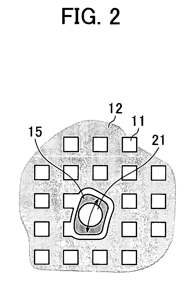
[0024] The chuck 1 has three small through-holes 15, through which pins 21 are able to pass in the Z direction to function as a support for the wafer 100. The pins 21 are f...

second embodiment

[0048]FIG. 5 shows an exposure system using the substrate holding device, according to the present invention, for fabricating a semiconductor device.

[0049] The exposure system is used for fabricating semiconductor devices, such as a semiconductor integrated circuit, a micromachine, and a device having a fine pattern, such as a thin film magnetic head. The exposure system forms a desired pattern on a substrate by projecting exposure light, which is exposure energy emitted from a light source 161, onto a semiconductor wafer or substrate 100 through a reticle R, which is an original plate, and through a projection lens unit 162. As used herein, the term “exposure light” is a general term used to denote, for example, visible light, ultraviolet light, EUV light, X-rays, electron beams, and charged particle beams, and the term “projection lens” is a general term used to denote, for example, a refractive lens, a reflector lens, a refractive and reflector lens system, and a lens for charge...

third embodiment

[0053] A fabrication process of a semiconductor device using the exposure system will now be described. FIG. 6 is a flow chart of all the fabrication steps for a semiconductor device. At step S1 (circuit design), the circuit of the semiconductor device is designed. At step S2 (mask making), a mask is created based on a designed circuit pattern.

[0054] At step S3 (wafer fabrication), a wafer is fabricated using a material, such as silicon. At step S4 (wafer process), which is referred to as “front end processing,” an actual circuit is formed on a wafer with the above-described exposure system by photolithography using the above-described mask. Subsequently, at step S5 (assembly), which is referred to as “back end processing,” the wafer processed at step S4 is turned into semiconductor chips. This step includes an assembly sub-step (dicing and bonding) and a packaging sub-step (chip encapsulation). At step S6 (test), a functioning test and a durability test of a semiconductor device f...


PUM

PropertyMeasurementUnit
holding forceaaaaaaaaaa
electrostatic forceaaaaaaaaaa
operating distanceaaaaaaaaaa

Abstract

A substrate holding device has a substrate holding unit and supporting elements movable to protrude from a substrate-holding surface of the substrate holding unit. The substrate holding unit holds the substrate in a predetermined state with a first holding force after relative positions of the substrate and the substrate holding unit are adjusted while the supporting elements lift the substrate off the substrate-holding surface. Before the relative positions of the substrate and the substrate holding unit are adjusted, the substrate holding device holds the substrate with a second holding force that is smaller than the first holding force and includes a zero holding force. Thus, the substrate holding device is able to align and hold the substrate in a short time.

Description

BACKGROUND OF THE INVENTION [0001] 1. Field of the Invention [0002] The present invention relates to a substrate holding device that holds a substrate, such as a wafer, during semiconductor fabrication and, in particular, a substrate holding device included in an exposure system for fabricating a semiconductor device. [0003] 2. Description of the Related Art [0004] An exposure system used in fabrication of a semiconductor device or a liquid crystal display device includes a substrate holding device that holds an original plate, such as a mask or a reticle, and a substrate, such as a semiconductor wafer or a glass substrate, which is an object to be exposed (hereinafter simply referred to as “a substrate”). [0005] Japanese Patent Laid-Open No. JP2001-044093 discloses an example of such a known substrate holding device. In general, a wafer transferred to a stage is coarsely pre-positioned, and is thereafter fine positioned. In the above-described publication, a wafer is transferred to...

Claims


Application Information

Patent Timeline
Patent Type & Authority Applications(United States)
IPC IPC(8): G03B27/58G03F7/20H01L21/027H01L21/68H01L21/683H02N13/00
CPCG03F7/70708G03F7/707
Inventor AKUTSU, KOTAROINOUE, MITSURU
Owner CANON KK
Why Eureka
Try Eureka