Optical modulating device, display, and exposure device

a technology of optical modulating device and exposure device, which is applied in the direction of optics, instruments, optical elements, etc., can solve the problems of low light utilization efficiency, deterioration of image quality, and existing flat display elements described above, so as to prevent a decrease in contrast, improve light utilization efficiency, and reduce cost

Inactive Publication Date: 2005-01-27
FUJIFILM HLDG CORP +1
View PDF2 Cites 35 Cited by
  • Summary
  • Abstract
  • Description
  • Claims
  • Application Information

AI Technical Summary

Benefits of technology

In this light-modulating element, since the light to be introduced into the light-modulating element is planar light, the loss in a light path is reduced and the planar incident light can be introduced into the light-modulating element at a high efficiency while retaining the planar state. A constitution having an elevated energy efficiency can hence be attained.
Consequently, light recycling occurs and the efficiency of light utilization is improved. Thus, a higher efficiency is attained.

Problems solved by technology

However, the existing flat display elements described above have the following problems.
First, the liquid-crystal display has a problem that since the light emitted by the backlight is caused to pass through many layers comprising the polarizers, transparent electrodes, and color filter, the efficiency of light utilization is low.
Other problems thereof include those characteristic of liquid crystals, i.e., deterioration in image quality due to viewing angle dependence and deterioration in dynamic-image quality due to a low response rate, and a cost problem in large displays employing a TFT.
The plasma display has drawbacks that since partition walls for discharge should be formed for each pixel, it is difficult to obtain high brightness at a high efficiency when the resolution is high, and that the display is costly because it necessitates a high operating voltage.
Furthermore, the FED has a drawback that the production cost is high as in the plasma display because the inside of the panels should be evacuated to an ultrahigh vacuum so as to enable a discharge to occur stably at a high efficiency.
The FED has further had a disadvantage that a high voltage is necessary for accelerating electrons resulting from field emission and causing these to strike on the phosphor.
Furthermore, since the positional change with voltage shows hysteresis, passive-matrix operation with high contrast is possible in a two-dimensional array constitution and an active element such as a TFT is unnecessary.
However, the lightguide plate / waveguide of a thin flat shape has a small edge area available for incidence and tends to have an impaired efficiency of coupling with incident light.
Moreover, since a further thickness reduction and a larger area are desired in lightguide plates and waveguides, the edge area available for incidence tends to decrease more and more and there is a fear of an impaired efficiency of coupling.
Furthermore, there are limitations on the shape of incident light (light source) and on position for introduction.
Namely, the size and number of light sources are limited and high-output light cannot be introduced.
In addition, the incident light should have a beam / linear shape and this poses limitations on the kind of light sources or separately necessitates an optical system for forming such shape.
As a result, there is a problem that the production process is complicated to increase the cost.
In the flat display element 80, when an element located upstream in the light path from the lightguide is brought into an ON state for image production, the light introduced into areas located downstream in the light path from this element attenuates to cause the so-called crosstalk and thereby impair image quality.
Furthermore, there also is a problem that leakage light released from an ON-state element reduces the contrast of images around the element.
On the other hand, in the flat display element 90, since high-output light is injected into the thin lightguide, a loss of light coupling occurs in the lightguide, resulting in a reduced efficiency of light utilization.
Furthermore, in case where the waveguide has even a slight defect in part thereof, leakage light is released from this part.

Method used


Image

  • Optical modulating device, display, and exposure device
  • Optical modulating device, display, and exposure device
  • Optical modulating device, display, and exposure device

Examples


second embodiment

the invention constituted by two-dimensionally arranging display elements described above will be explained below by means of FIG. 12 and FIG. 13.

FIG. 12 is a plan view of a flat display element comprising two-dimensionally arranged display elements employing a flexible this film. FIG. 13 is sectional views taken on C-C of FIG. 12; (a) is a view illustrating the OFF state and (b) is a view illustrating the ON state.

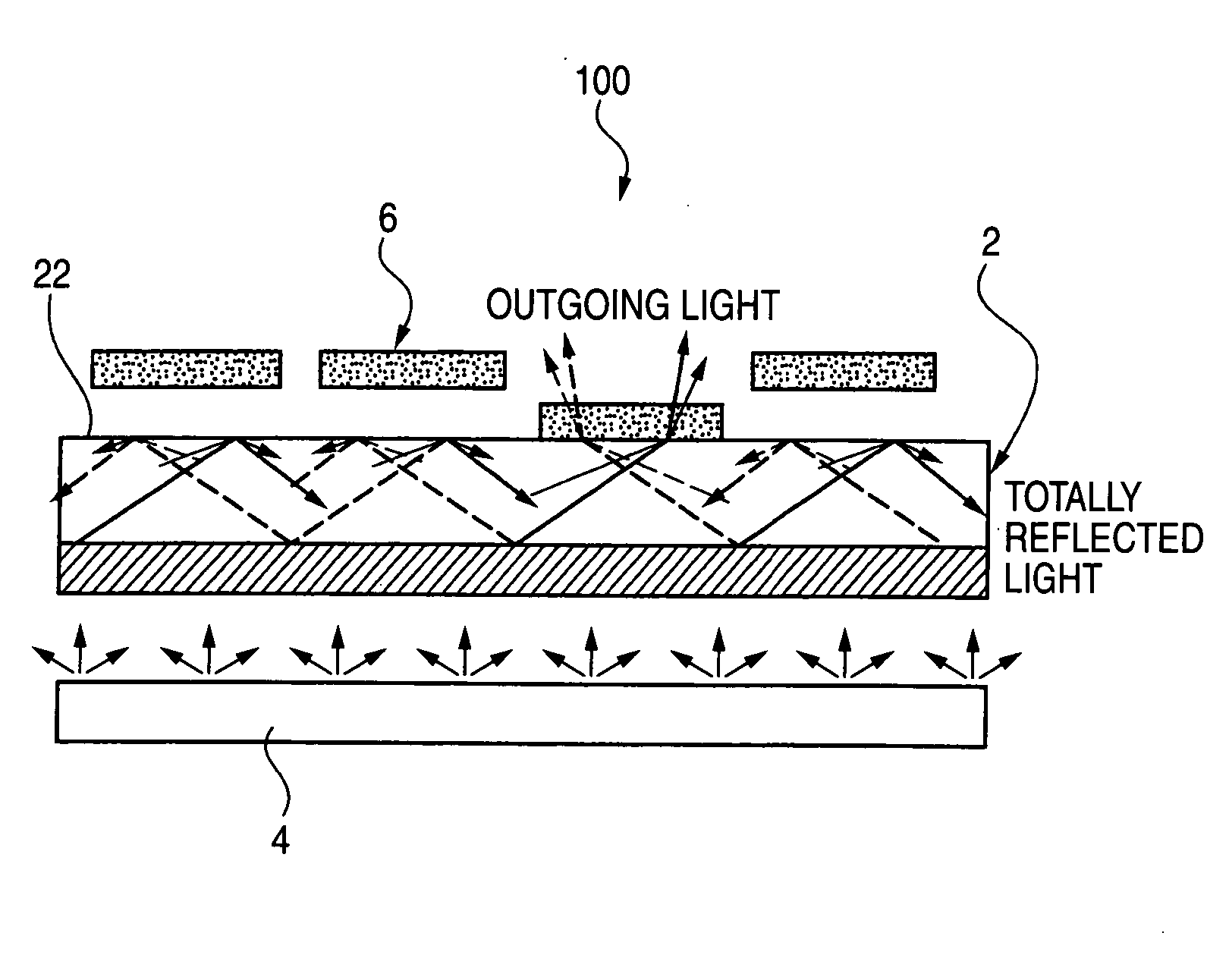
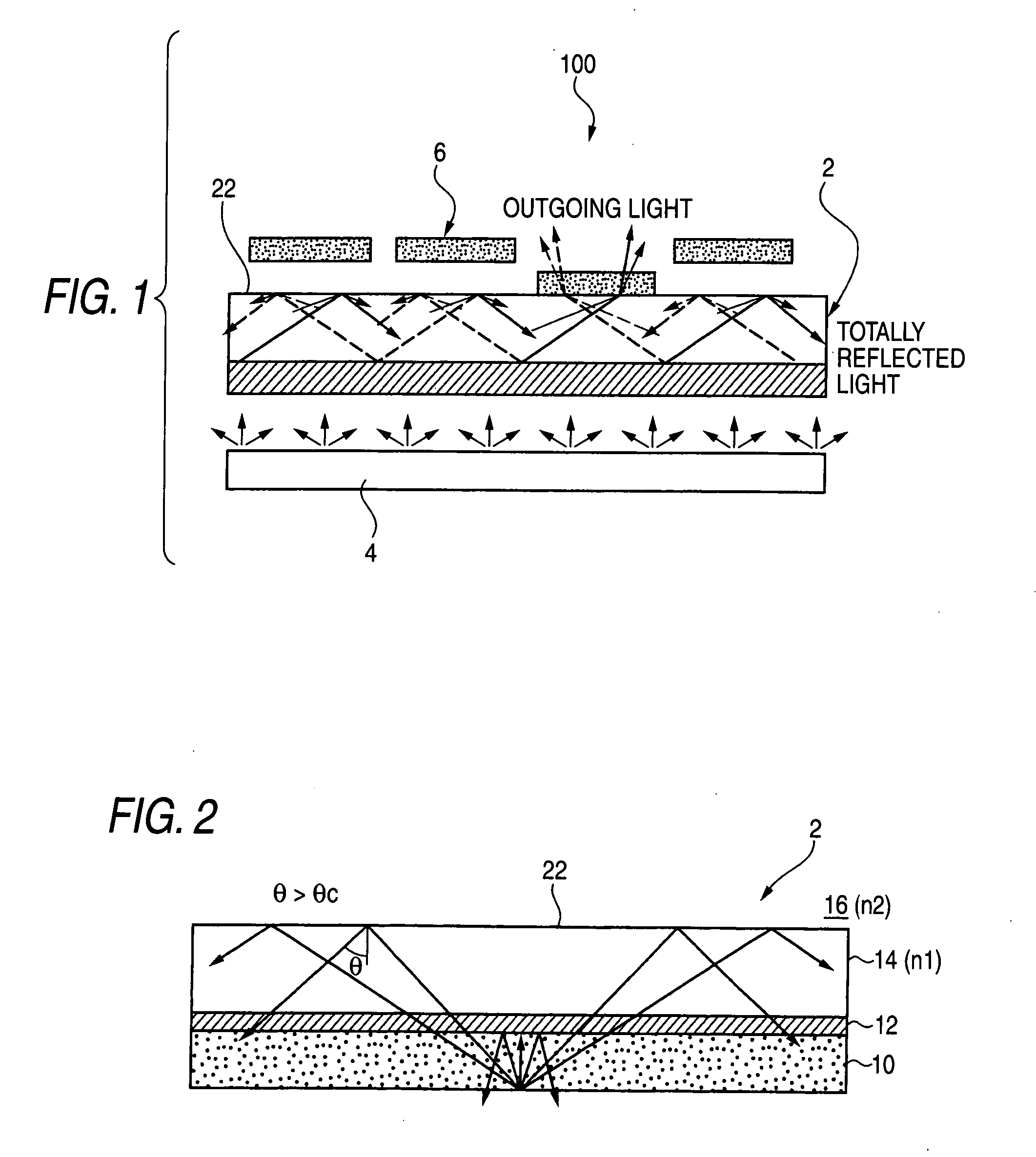
As shown in FIG. 12 and FIG. 13, the flat display element 200 according to this embodiment comprises a total-reflection optical member 2 and light-coupling elements 6 disposed over the total reflection plane 22 of the optical member 2 in two-dimensional arrangement with m lines and n rows (m and n are integers). Specifically, signal electrodes 32 transparent to incident light have been arranged in parallel in the row direction so as to constitute n rows over the total reflection plane 22, and scanning electrodes 34 likewise transparent to incident light have been arrang...

fourth embodiment

the invention in which ultraviolet is modulated with the display element of the invention to cause phosphors to show excitation luminescence will be explained below.

FIG. 16 is sectional views illustrating part of an excitation luminescence type flat display element according to this embodiment which includes a flexible thin film and formed thereon the phosphors of the excitation luminescence type flat display element described above; (a) is a view illustrating the OFF state and (b) is a view illustrating the ON state.

As shown in FIG. 16(a), the excitation luminescence type flat display element 400 according to this embodiment has no front-side plate and has phosphors 52a, 52b, and 52c directly formed on the flexible thin film 40. Thus, the constitution and molding step have been simplified, and a further reduction in thickness and a cost reduction are attained. The phosphors 52a, 52b, and 52c are partitioned by a black matrix to thereby enhance the contrast of display images.

In ...


PUM

PropertyMeasurementUnit
refractive indexaaaaaaaaaa
wavelengthsaaaaaaaaaa

Abstract

Subjects for the invention are to provide a light-modulating element having an elevated energy efficiency while preventing a decrease in contrast at low cost without using a display technique employing a waveguide or lightguide plate, and to provide a display element capable of producing high-quality display images and an exposure element capable of exposure treatment. In the invention, the light-modulating element comprises: a total-reflection optical member 2 having such a property that at least part of planar incident light introduced into the light-modulating element is totally reflected at an interface (total reflection plane) 22 of a layer constituted by the light-modulating element and the incident light does not substantially go out through the side opposite to the incident-light introduction side; and light-coupling elements 6 which are disposed on the total reflection plane 22 side of the total-reflection optical member 2 and serve to selectively couple with the incident light and take out the same from the total reflection plane 22.

Description

TECHNICAL FIELD The present invention relates to a flat light-modulating element and display element into which planar incident light is introduced to produce a desired image, and also to an exposure element. BACKGROUND ART Among devices in which incident light is regulated with respect to amplitude (intensity), phase, direction of traveling, or the like to process / exhibit an image or patterned data is a light-modulating element. In a light-modulating element, the refractive index of a substance which transmits light is changed by means of an external field applied to the substance and the intensity of the light which finally passes through or is reflected by this substance is controlled through an optical phenomenon such as refraction, diffraction, absorption, or scattering. Examples of this light-modulating element include liquid-crystal light-modulating elements which utilize an electrochemical effect of a liquid crystal. Such liquid-crystal light-modulating elements are being ...

Claims


Application Information

Patent Timeline
Patent Type & Authority Applications(United States)
IPC IPC(8): G02B26/02G02B26/08G02F1/13G02F1/1333G02F1/13357G02F1/315
CPCG02B26/02G02F1/315G02F1/1326G02F1/13
Inventor KIMURA, KOICHI
Owner FUJIFILM HLDG CORP
Why Eureka
Try Eureka