Traveling-wave optoelectronic wavelength converter

a wavelength converter and optoelectronic technology, applied in the field of microelectronic and optoelectronic components, can solve the problems of limiting the operation bandwidth, large capacitance, and severe limitations, and achieve the effects of improving the efficiency and signal bandwidth, modulation extinction, and output optical signal level or wavelength conversion efficiency

Inactive Publication Date: 2005-01-27
JDS UNIPHASE CORP
View PDF9 Cites 9 Cited by
  • Summary
  • Abstract
  • Description
  • Claims
  • Application Information

AI Technical Summary

Benefits of technology

[0012] The present invention describes a monolithic wavelength converter assembly that provides for optical signal regeneration or amplification without using electronic circuits. The monolithic wavelength converter assembly uses a common layer structure and includes a widely-tunable laser and interconnected traveling-wave photodetector (TWPD) and traveling-wave modulator (TWM) for improved efficiency and si

Problems solved by technology

This can be severely limited because the lengths of both the photodetector and modulator need to be relatively long for efficient operation, and this results in a relatively large capacitance.
Thus, RL must be as large as possible for efficient wavelength conversion, but this limits the bandwidth of operation.
Therefore, there is a severe trade-

Method used


Image

  • Traveling-wave optoelectronic wavelength converter
  • Traveling-wave optoelectronic wavelength converter
  • Traveling-wave optoelectronic wavelength converter

Examples


embodiments

[0030] Embodiments

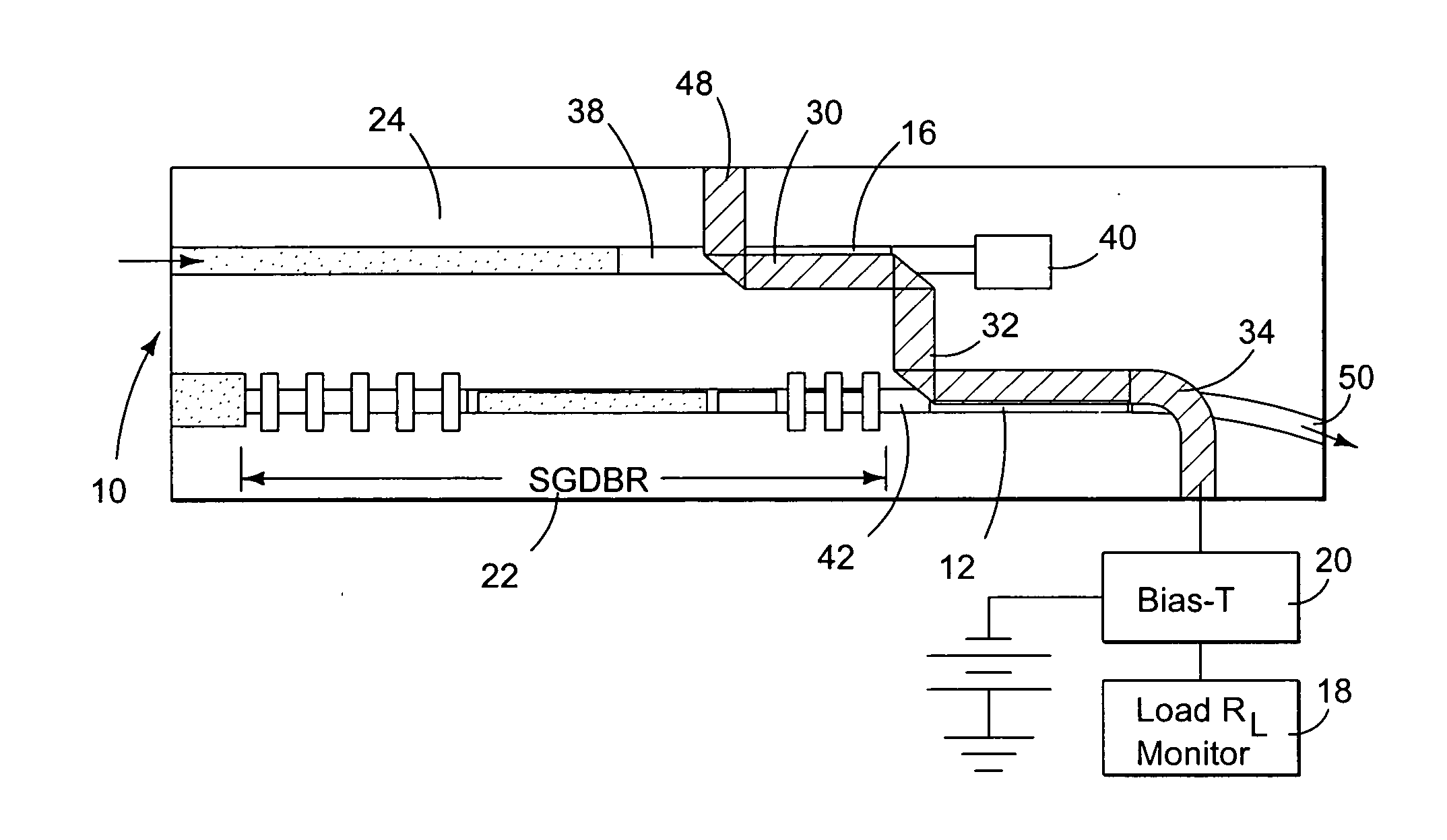
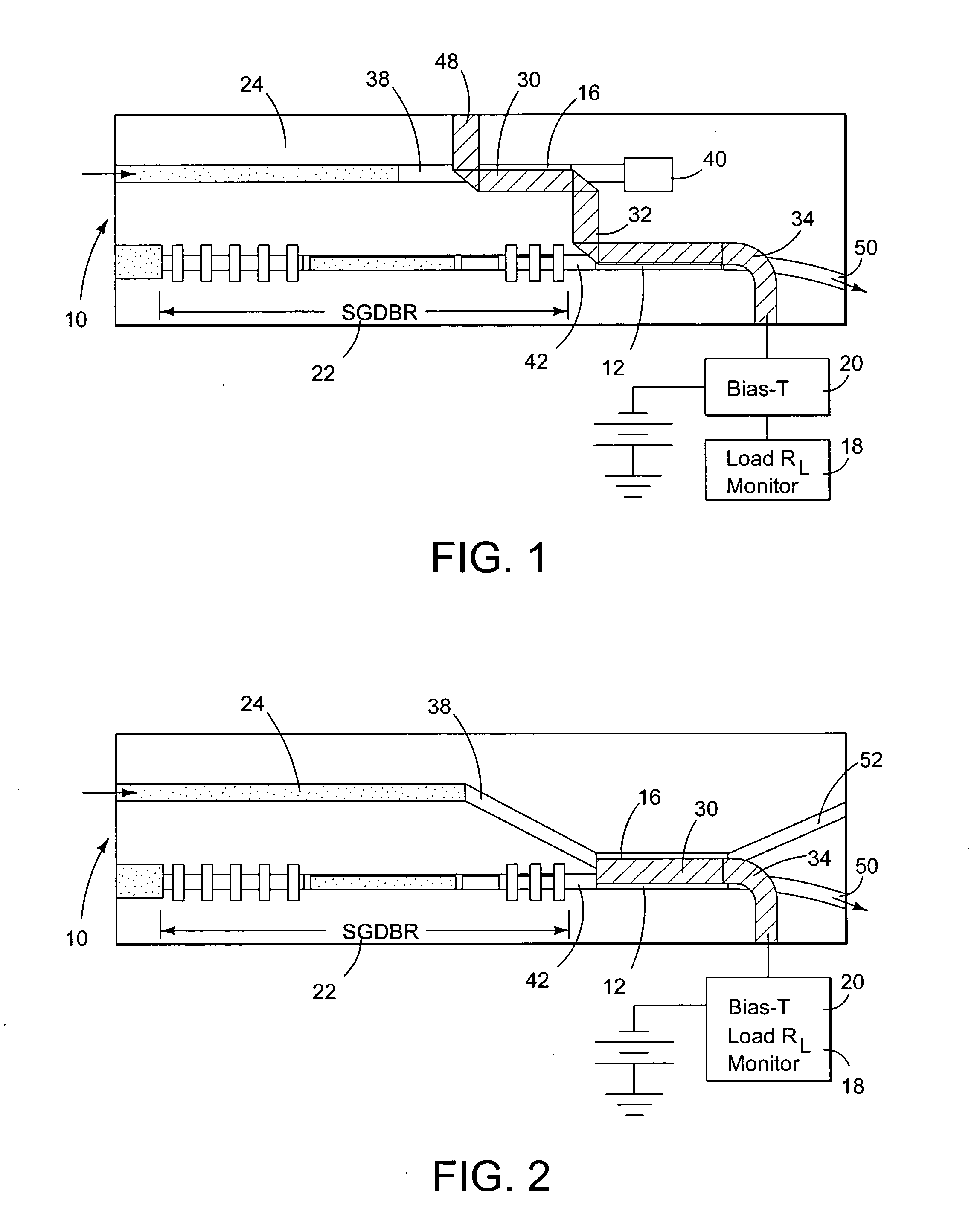
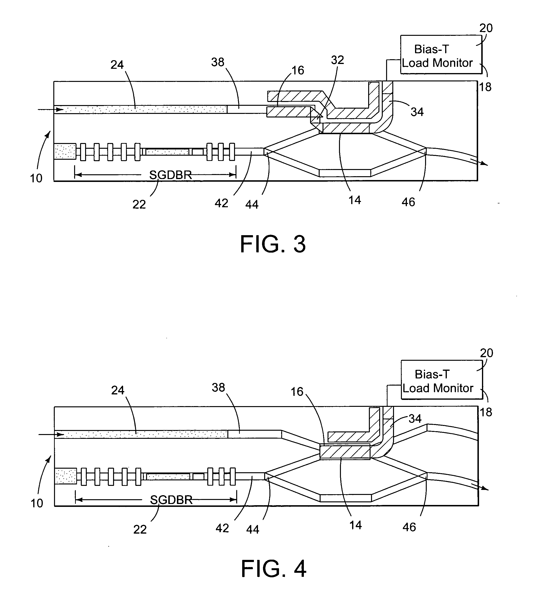
[0031]FIGS. 1-5 illustrate five embodiments of traveling-wave optoelectronic wavelength converter assemblies 10 that provide for increased operating bandwidth with higher efficiency than possible with lump-element wavelength converters. FIGS. 1 and 2 employ a traveling-wave electro-absorption modulator (TWEAM) 12, and FIGS. 3, 4 and 5 employ a traveling-wave Mach-Zehnder interferometric modulator (TWMZM) 14. The TWEAM 12 has a smaller footprint and may require lower voltages, while the TWMZM 14 allows for better chirp control and can provide more output power. The TWEAM 12 and TWMZM 14 are generically referred to as a traveling-wave modulator (TWM) 12, 14.

[0032]FIGS. 1 and 3 use a series connection of the traveling-wave photodetector (TWPD) 16 and TWM 12, 14 elements, while FIGS. 2, 4 and 5 use a parallel connection of these elements. The series connection allows for separate optimization of the characteristic impedances of the TWPD 16, the TWM 12, 14, and the ele...

second embodiment

[0054] In FIG. 5, a parallel-connected optoelectronic wavelength converter assembly is shown, including a higher-impedance electrical transmission line 34 between the TWPD 16 and TWMZM 14, as well as a linearized SOA 24 acting as a preamplifier. By segmenting the contacts to the TWPD 16 and TWMZM 14, and by connecting them to the common high-impedance electrical transmission line 34 running therebetween, a higher overall transmission line 34 impedance is provided, and this will increase the propagating voltage magnitude for better wavelength conversion efficiency.

[0055] The SOA 24 in this case is linearized by including a grating 54 on its output side to provide for lasing at a wavelength that is somewhat shorter than the range of input signal wavelengths. This clamps the carrier density in the SOA 24, and thereby makes its gain insensitive to the level of the input signal.

[0056]FIGS. 7a-b and 8a-b again represent the electrical transmission line aspects for the cases of FIG. 3 and...


PUM


Abstract

Traveling-wave optoelectronic wavelength conversion is provided by a monolithic optoelectronic integrated circuit that includes an interconnected traveling-wave photodetector and traveling-wave optical modulator with a widely tunable laser source. Either parallel and series connections between the photodetector and modulator may be used. An input signal modulated onto a first optical wavelength develops a traveling wave voltage on transmission line electrodes of the traveling-wave photodetector, and this voltage is coupled via an interconnecting transmission line of the same characteristic impedance to transmission line electrodes of the traveling-wave optical modulator to modulate the signal onto a second optical wavelength derived from the tunable laser. The traveling wave voltage is terminated in a load resistor having the same characteristic impedance as the photodetector and modulator transmission lines. However, the interconnecting transmission lines and the load resistor may have different impedances than the photodetector and modulator.

Description

CROSS-REFERENCE TO RELATED APPLICATIONS [0001] This application claims the benefit under 35 U.S.C. §119(e) of co-pending and commonly-assigned U.S. provisional patent application Ser. No. 60 / 490,046, filed Jul. 25, 2003, by Christopher W. Coldren and Larry A. Coldren, and entitled “TRAVELING-WAVE OPTOELECTRONIC WAVELENGTH CONVERTER,” which application is incorporated by reference herein.BACKGROUND OF THE INVENTION [0002] 1. Field of the Invention [0003] This invention relates to microelectronic and optoelectronic components, and more particularly, to a traveling-wave optoelectronic wavelength converter. [0004] 2. Description of the Related Art [0005] (Note: This application incorporates a number of different references as indicated throughout the specification by numbers enclosed in brackets, e.g., [x]. A list of these different references ordered according to these numbers can be found below in the section of the specification entitled “References.” Each of these references is inco...

Claims


Application Information

Patent Timeline
IPC IPC(8): G02F1/035G02F1/225G02F2/00
CPCB82Y20/00H01S5/1209G02F1/0356G02F1/2255G02F1/2257G02F2/004G02F2001/212G02F2002/008G02F2201/127H01L31/035236H01L31/105H01S5/026H01S5/0262H01S5/0265H01S5/0427H01S5/06256G02F1/025G02F1/212G02F2/008
Inventor COLDREN, CHRISTOPHER W.COLDREN, LARRY A.
Owner JDS UNIPHASE CORP
Why Eureka
Try Eureka