High speed and wide viewing angle liquid crystal displays

Inactive Publication Date: 2005-02-03
UNIV OF CENT FLORIDA RES FOUND INC +1
View PDF6 Cites 73 Cited by
  • Summary
  • Abstract
  • Description
  • Claims
  • Application Information

AI Technical Summary

Benefits of technology

[0012] The first objective of the present invention is to provide configurations and methods for usin

Problems solved by technology

Slow response time and poor viewing angle of the conventional TFT-LCD are two of the major limitations for its otherwise potentially unlimited wide range of applications.
With only one type of electric field generated, this results in a very slow relaxation and hence slow turn off time, and is a major limitation of liquid crystals for many potential applications today.
The liquid crystal displays employing the crossed-field effect have various disadvantages, such as, high voltage requirement, low contrast, more complicated structure, non-uniform transmission, and more complicated driving.
Some driving schemes are more complicated, e

Method used


Image

  • High speed and wide viewing angle liquid crystal displays
  • High speed and wide viewing angle liquid crystal displays
  • High speed and wide viewing angle liquid crystal displays

Examples


Example

EXAMPLE 1

Lower Voltage for One Common Electrode

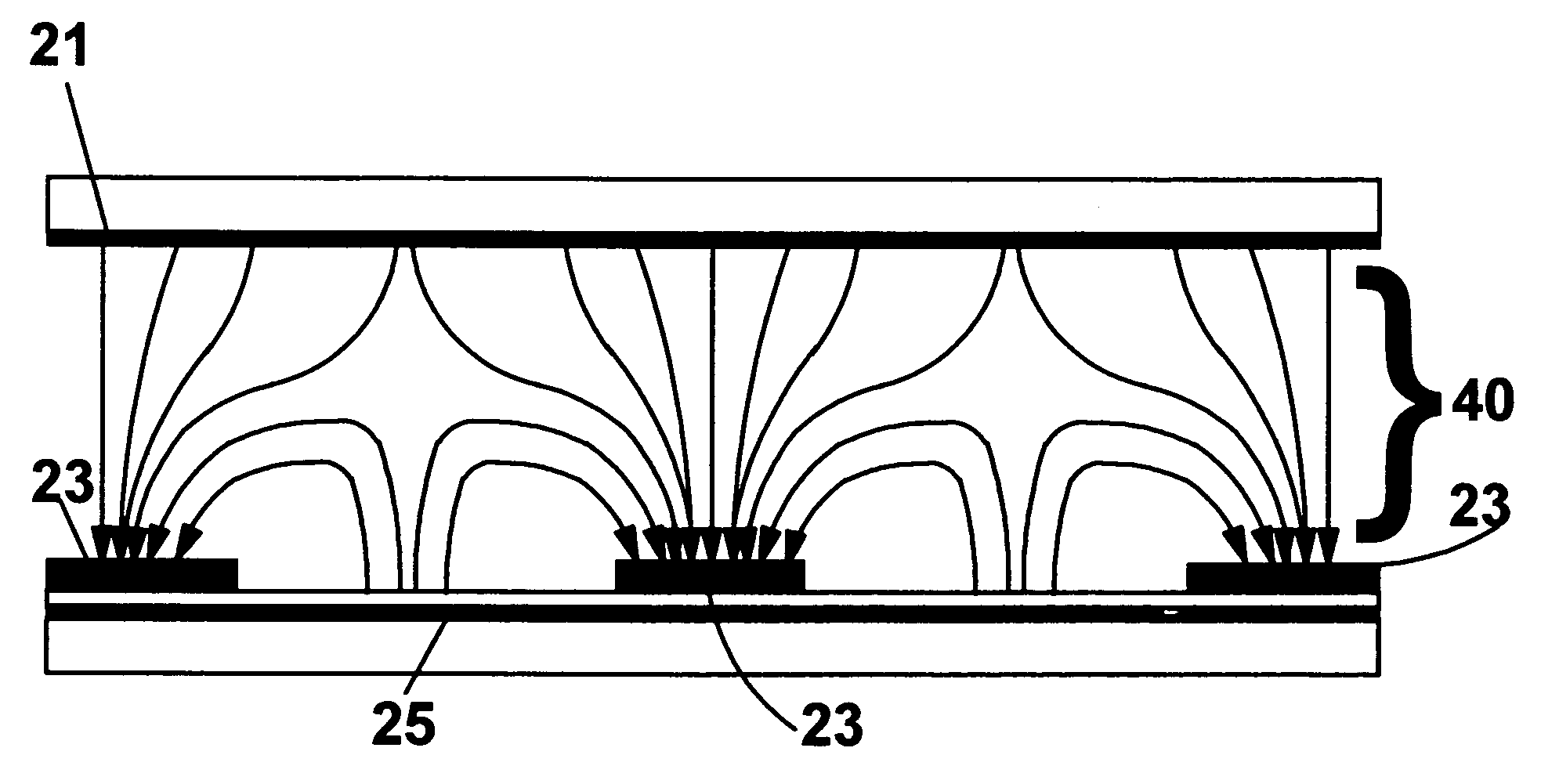
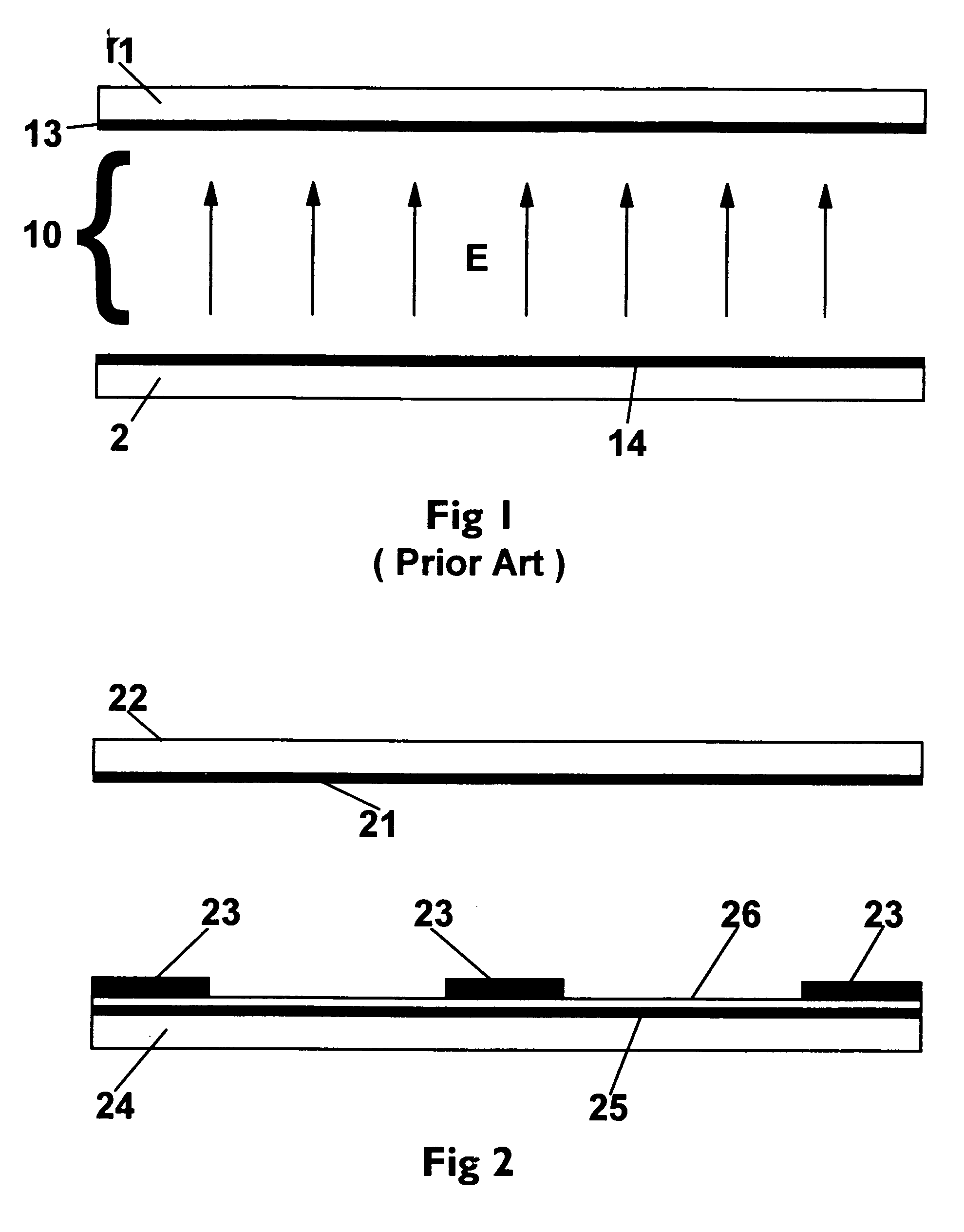
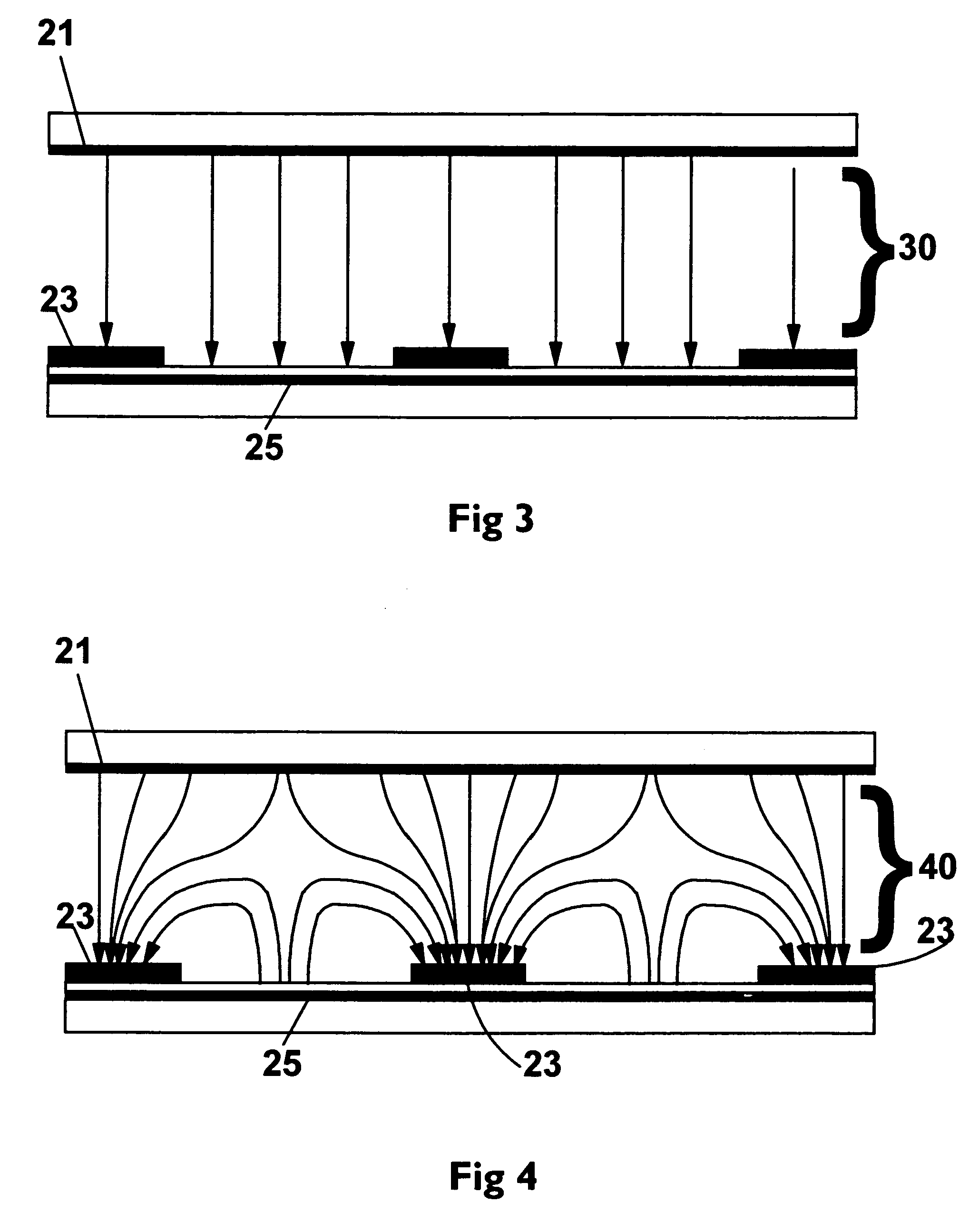
[0034] The voltage for common electrode 21 in FIG. 2 is 5V; this voltage can be made lower in order to reduce the vertical electric field strength and hence strengthen the lateral field. This can help improve the light efficiency since the lateral field becomes stronger and more molecules are switched to the bright state. This will however increase the corresponding response time for the bright-to-dark state due to the formation of a weaker vertical field. The remaining voltage readings are for common electrode 23 on bottom substrate 24, V=0V; for pixel electrode 25 V=0 to 5V. Common electrode 23 is electrically insulated from the pixel electrode 25 by a passivation layer 26.

Example

EXAMPLE 2

Higher Voltage to Bottom Electrode

[0035] In FIG. 2, common electrode 21 has higher voltage; whereas, common electrode 23 has lower voltage and in principle these two electrodes can be interchanged. This interchange is shown in FIG. 5. In FIG. 5, the first common electrode 51 on top substrate 52 has a lower voltage (0V); whereas the second common electrode layer 53 in the bottom substrate 54 has a higher voltage (5V). This alternative design may lead to a less uniform vertical field because of the slightly higher potential difference that is caused by the passivation layer 56. In FIG. 5, a high electric field is emitted from pixel electrode 55 and hence a higher electric field is established across the passivation layer 56 than when the electric field is emitted from the top electrode 51. It should be noted, that the terminology “passivation layer” in the description of the present invention, is commonly known as an insulation layer. However, the potential difference that ...

Example

EXAMPLE 3

Common Electrode and Pixel Electrode Interchanged

[0036] A first common electrode layer 60 with 5V is in top substrate 61 as shown in FIG. 6. The bottom substrate 63 supports a pixel electrode layer 62 with 0 to 5V and a second common electrode layer 64 with 0V. The pixel electrode layer 62 is electrically insulated from the common electrode 64 by a passivation layer 65. The positions of common electrode 64 and the pixel electrode 62 in this configuration are interchanged compared with the configuration shown in FIG. 2. The choice of the configuration depends on the fabrication process capability and the optimized electrode width and gap.


PUM


Abstract

Novel structural configurations of a TFT-LCD (Thin Film Transistor Liquid Crystal Display) which results in both fast response to input data and provides wide-viewing-angles. The structure of the device is comprised of one pixel electrode layer and two common electrode layers. The structure of the invention can be used with liquid crystal display television (LCD-TV) monitors that require both fast-response as well as wide-viewing-angle. In addition, other liquid crystal technologies which require high speed response would benefit from the TFT-LCD of the present invention.

Description

[0001] This invention claims the benefit of priority to U.S. Provisional Application No. 60 / 405,999 filed Aug. 26, 2002.FIELD OF INVENTION [0002] This invention relates to displays, in particular to methods and apparatus for providing a TFT-LCD (Thin Film Transistor Liquid Crystal Display) having fast responses to high input data rates and allowing for wide viewing angles for viewers. BACKGROUND AND PRIOR ART [0003] Slow response time and poor viewing angle of the conventional TFT-LCD are two of the major limitations for its otherwise potentially unlimited wide range of applications. [0004]FIG. 1 shows the structure of a conventional TFT-LCD. A liquid crystal (LC) layer 10 is sandwiched between a top glass substrate 11 and a bottom glass substrate 12. A thin layer of transparent electrode, indium tin oxide (ITO), is coated on each substrate for the application of an electric field to switch the liquid crystals. Normally, the electrode 13 for the top substrate 11 is a common electrod...

Claims


Application Information

Patent Timeline
IPC IPC(8): G02F1/1343
CPCG02F2001/134381G02F1/134363G02F1/134381
Inventor CHOI, WING-KITWU, SHIN-TSON
Owner UNIV OF CENT FLORIDA RES FOUND INC
Why Eureka
Try Eureka