

Lithographic antireflective hardmask compositions and uses thereof
a technology of antireflective hardmasks and compositions, applied in the field of semiconductor devices, can solve the problems of poor etch selectivity of arc materials on imaging layers, insufficient resistance to subsequent etching steps, and a large amount of imaging layers consumed
- Summary
- Abstract
- Description
- Claims
- Application Information
AI Technical Summary
Problems solved by technology
Method used
Image

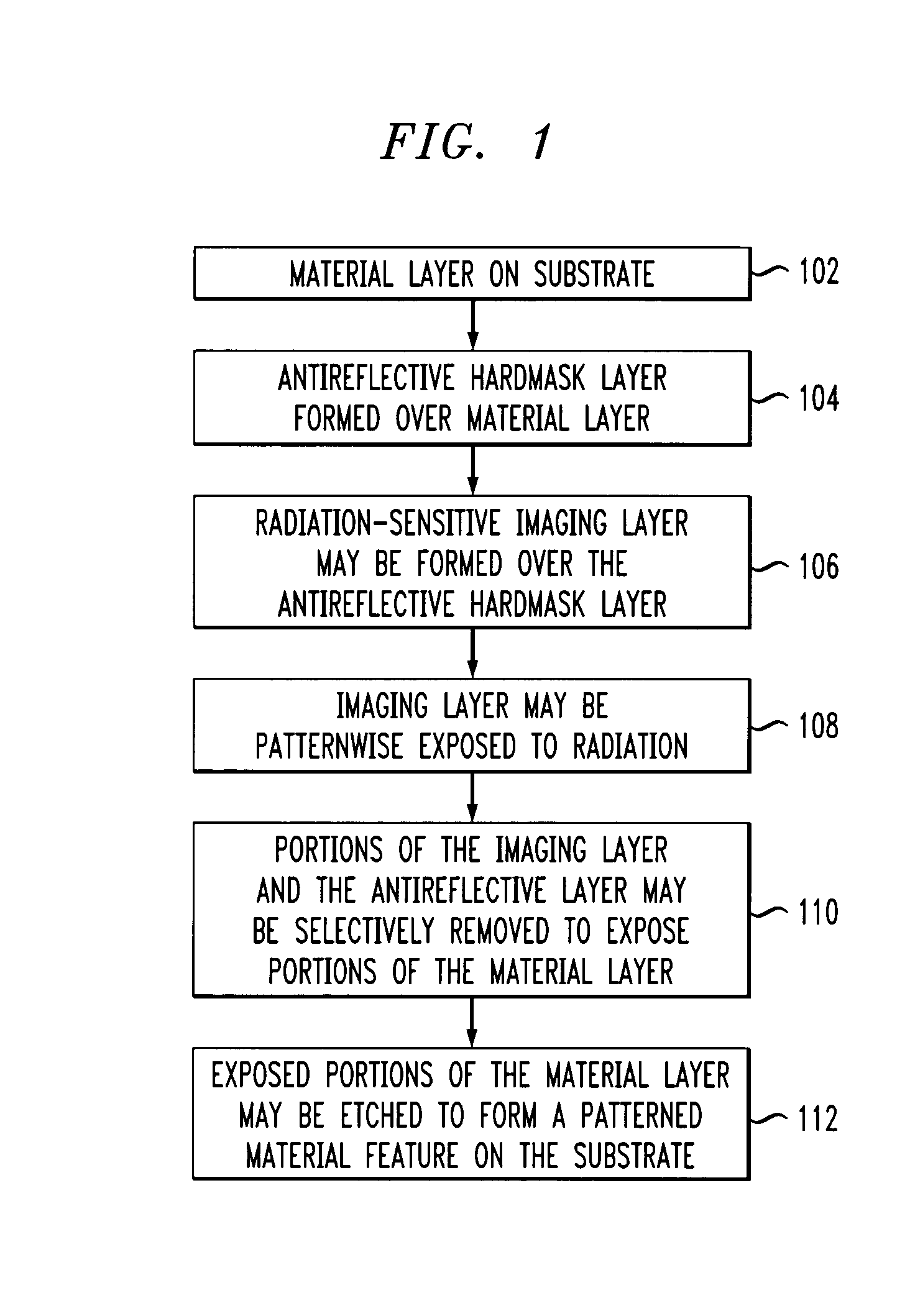
Examples
example 1
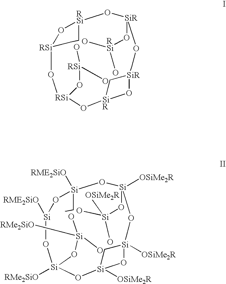
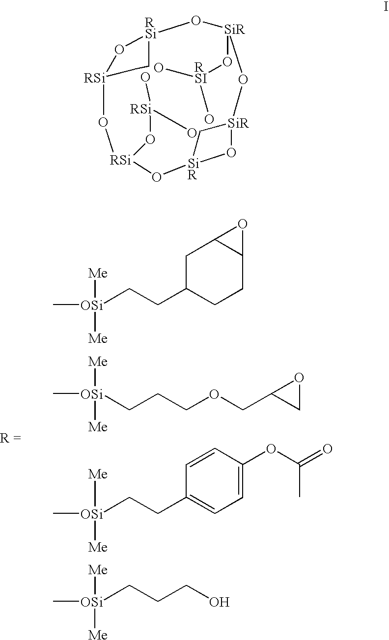
The POSS materials Octakis {(glycidoxypropyl)dimethylsiloxy}silsesquioxane, Octakis {(ethylcyclohexylpropyl)dimethylsiloxy}silsesquioxane, Octakis {(propanol)dimethylsiloxy}silsesquioxane and Octakis {(ethylphenylacetate)dimethylsiloxy}silsesquioxane were obtained from TAL Materials, Inc.
example 2
Formulation
The desired POSS material from Example 1 was dissolved in propylene glycol monomethyl ether acetate (PGMEA) or ethyl lactate in concentrations of 12 percent by weight to the solvent to 14 percent by weight to the solvent. A crosslinking agent tetramethoxymethyl glycoluril, available from DayChem, in a concentration of eight parts by weight relative to POSS and di(t-butylphenyl)iodoniumperfluorobutylsulfonate (DtBPI-PFBuS) in a concentration of four parts by weight relative to POSS were added to the solution.
example 3
Film Formation and Optical Properties
Formulations POSS A, POSS B, POSS C and POSS D comprising Octakis {(glycidoxypropyl)dimethylsiloxy}silsesquioxane, Octakis {(ethylcyclohexylpropyl)dimethylsiloxy}silsesquioxane, Octakis {(propanol)dimethylsiloxy}silsesquioxane and Octakis {(ethylphenylacetate)dimethylsiloxy}silsesquioxane, respectively, prepared as described in Example 2, were spin coated onto a 200 millimeter silicon wafer at 3,000 revolutions per minute for 60 seconds. The film thicknesses ranged from 1,700 to 2,500 angstroms. The spin cast film was cured at 200° C. for 60 seconds. The optical constants, the index of refraction n and the extinction coefficient k at 193 nm, were measured using an n&k Analyzer manufactured by n&k Technology, Inc.
The optical properties of the films for 193 nm radiation were as follows:
Film POSSnKPOSS A1.6110.030POSS B1.6450.050POSS C1.6470.026POSS D1.6890.205POSS A & D (4:1 wt / wt)1.7350.278POSS B & D (4:1 wt / wt)1.7620.308
PUM
| Property | Measurement | Unit |
|---|---|---|
| transparent | aaaaa | aaaaa |
| wavelength | aaaaa | aaaaa |
| thickness | aaaaa | aaaaa |
Abstract
Description
Claims
Application Information