Method and apparatus for forming silicon-containing insulation film having low dielectric constant

a technology of dielectric constant and insulation film, which is applied in the direction of coating, chemical vapor deposition coating, plasma technique, etc., can solve the problems of low heat resistance, poor adhesion to silicon materials, and expensive devices used for curing process after coating materials. achieve the effect of low dielectric constant and high mechanical strength

Active Publication Date: 2005-02-17
ASM JAPAN
View PDF15 Cites 37 Cited by
  • Summary
  • Abstract
  • Description
  • Claims
  • Application Information

AI Technical Summary

Benefits of technology

[0015] In view of the above-mentioned problems, an object of the present invention is to provide a method and an apparatus for forming an insulation film having a low dielectric constant and high mechanical strength.

Problems solved by technology

However, the above-mentioned conventional approaches have the following problems:
In the case of the inorganic SOG insulation film formed by the spin-coat method, there are problems in that the materials properties are not distributed equally on a silicon substrate and that a device used for a curing process after coating the material is expensive.
In the case of the fluorinated amorphous carbon film by the plasma CVD method using CxFyHz as a source gas, there are problems such as low heat resistance (370° C.
), poor adhesion with silicon materials, and low mechanical strength of the film formed.
Furthermore, among silicon-containing hydrocarbons, when P-TMOS is used, a polymerized oligomer cannot form a linear structure such as a siloxane polymer because P-TMOS contains three alkoxy groups.
Consequently, a porous structure is not formed on a silicon substrate, and hence a dielectric constant cannot be reduced to a desired degree.
However, there are problems in that oligomers having the linear structure have weak bonding power therebetween and thus the mechanical strength of a resultant film is low.

Method used


Image

  • Method and apparatus for forming silicon-containing insulation film having low dielectric constant
  • Method and apparatus for forming silicon-containing insulation film having low dielectric constant
  • Method and apparatus for forming silicon-containing insulation film having low dielectric constant

Examples


examples

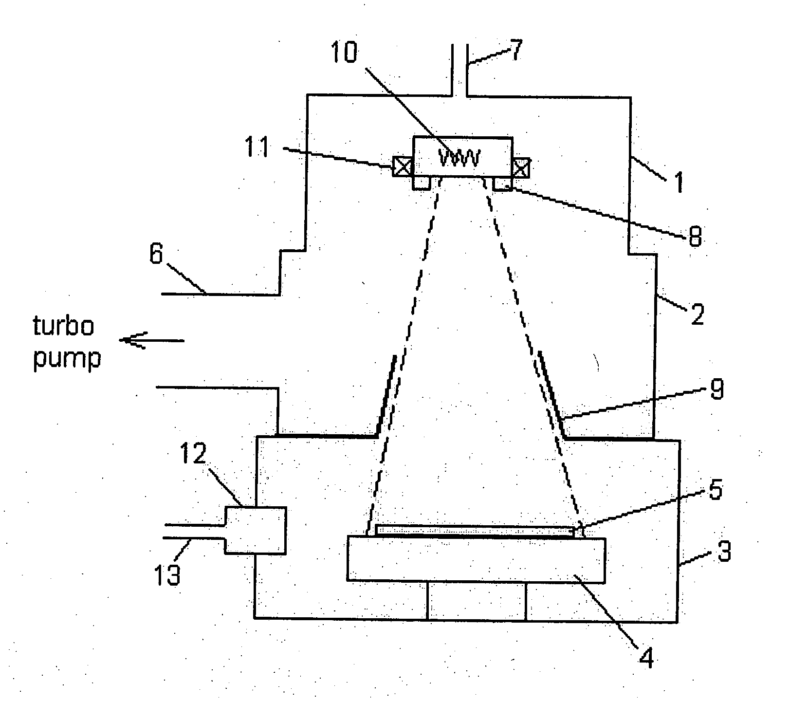
[0088] Preferred embodiments of the method for forming a silicon-containing insulation film having a low dielectric constant and high mechanical strength according to the present invention are described below.

[0089] Before starting descriptions, a simple calculating formula of a scanning depth of electron beam is explained.

[0090] According to “S. Schiller, Electron Beam Technology, by John Wiley & Sons, (1983)”,

S=0.0667V5 / 3 / ρ[0091] S: Electron Path vertical to material surface (μm) [0092] V: Accelerating voltage (kV) [0093]ρ: Density (g / cm3)

[0094] From this formula, it is seen that changing an accelerating voltage is required per film thickness processed and film density.

[0095] It is seen that: When film density is 0.9 g / cm3, accelerating voltage is 2.3 kV for a film thickness of 300 nm, 3.2 kV for 500 nm, and 7.3 kV for 2000 nm; when film density is 1.8 g / cm3, accelerating voltage is 3.6 kV for a film thickness of 300 nm, 4.8 kV for 500 nm, and 11 kV for 2000 nm; and the optimu...


PUM

PropertyMeasurementUnit
elastic modulusaaaaaaaaaa
dielectric constantaaaaaaaaaa

Abstract

A silicon-containing insulation film is formed on a substrate by plasma reaction using a reaction gas including (i) a source gas comprising a silicon-containing hydrocarbon compound containing multiple cross-linkable groups, (ii) a cross-linking gas, and (iii) an inert gas, into a reaction chamber where a substrate is placed. The insulation film is then exposed to electron beam radiation, thereby increasing mechanical strength of the film without substantial alternation of its dielectric constant.

Description

BACKGROUND OF THE INVENTION [0001] 1. Field of the Invention [0002] The present invention relates to a method and an apparatus for forming a silicon-containing insulation film having a low dielectric constant. [0003] 2. Description of the Related Art [0004] As semiconductors have progressed to accommodate a demand for high speed and high density in recent years, a reduction of capacitance between lines is required to avoid signal delays in the multi-layer wiring technology field. Because a reduction in the dielectric constant of a multi-layer wiring insulation film is required in order to reduce the capacitance between lines, insulation films having low dielectric constants have been developed. [0005] Conventionally, silicon oxide (SiOx) film is formed by adding oxygen (O2) or nitric oxide (N2O) as an oxidizing agent to a silicon source gas such as SiH4 and Si(OC2H5)4 and applying heat or plasma energy to the source gas. A dielectric constant (∈) of this film was approximately 4.0. ...

Claims


Application Information

Patent Timeline
Patent Type & Authority Applications(United States)
IPC IPC(8): C23C16/40C23C16/505C23C16/42C23C16/56H01J37/32H01L21/31H01L21/312H01L21/316
CPCC23C16/401C23C16/505C23C16/56H01J37/32082H01L21/31612H01L21/02126H01L21/02208H01L21/02274H01L21/02351H01J37/3233H01L21/31
Inventor TSUJI, NAOTOFUKAZAWA, ATSUKIMATSUKI, NOBUOIKEDA, SHINGO
Owner ASM JAPAN
Why Eureka
Try Eureka