Beam irradiation apparatus, beam irradiation method, and method for manufacturing semiconductor device

a beam irradiation and beam technology, applied in the direction of laser beam welding apparatus, manufacturing tools, solid-state devices, etc., can solve the problems of difficult laser processing uniformity, inconvenient manufacturing of display devices, and inability to meet the requirements of laser processing uniformity, so as to achieve the effect of enhancing mass productivity and reducing cos

Active Publication Date: 2005-02-17
SEMICON ENERGY LAB CO LTD
View PDF23 Cites 32 Cited by
  • Summary
  • Abstract
  • Description
  • Claims
  • Application Information

AI Technical Summary

Benefits of technology

[0038] In the present invention, the beam can be irradiated uniformly by irradiating the beam to the outside of the display device, which is the outside of the element-forming region, when the CW beam is employed and when the scanning speed of the beam is not uniform. In other words, the laser annealing with the laser used as the light source can be performed uniformly. As a result, mass productivity is enhanced and the display device can be manufactured at lower cost.
[0039] Uniform processing can be performed by using the scanning means of the present invention in which the CW beam or the pulsed beam scanned on the irradiated object is irradiated to the outside of the element-forming region when the scanning direction of the laser beam changes or when the scanning speed is not constant. As a result, the semiconductor film can be annealed uniformly. As above, it is possible to prevent the irradiated object, particularly the semiconductor film, from being peeled. In addition, the efficient laser annealing of the present invention is preferable in the case of using the large substrate.

Problems solved by technology

The region where the scanning of the laser light stops makes it difficult to perform the laser processing uniformly.
Furthermore, the speed of the laser light scanned by the scanning means such as the galvanometer mirror or the polygon mirror was not constant in the center portion and in the end portion of the scanning width.
In such regions where the scanning speed decelerates, accelerates, and becomes zero, the irradiation time becomes longer so that the object is irradiated with excessive energy.
As a result, when the amorphous semiconductor film is used as the irradiated object, there is a risk that the amorphous semiconductor film is peeled or the like.
As a result, there is also a risk, as well as the galvanometer mirror, that the amorphous semiconductor film is peeled or the like.
It is concerned that when the semiconductor film is peeled, the peeled film is spattered to the normal film, which results in the roughness of the normal film.

Method used


Image

  • Beam irradiation apparatus, beam irradiation method, and method for manufacturing semiconductor device
  • Beam irradiation apparatus, beam irradiation method, and method for manufacturing semiconductor device
  • Beam irradiation apparatus, beam irradiation method, and method for manufacturing semiconductor device

Examples


embodiment

[0048] Embodiment Mode 1

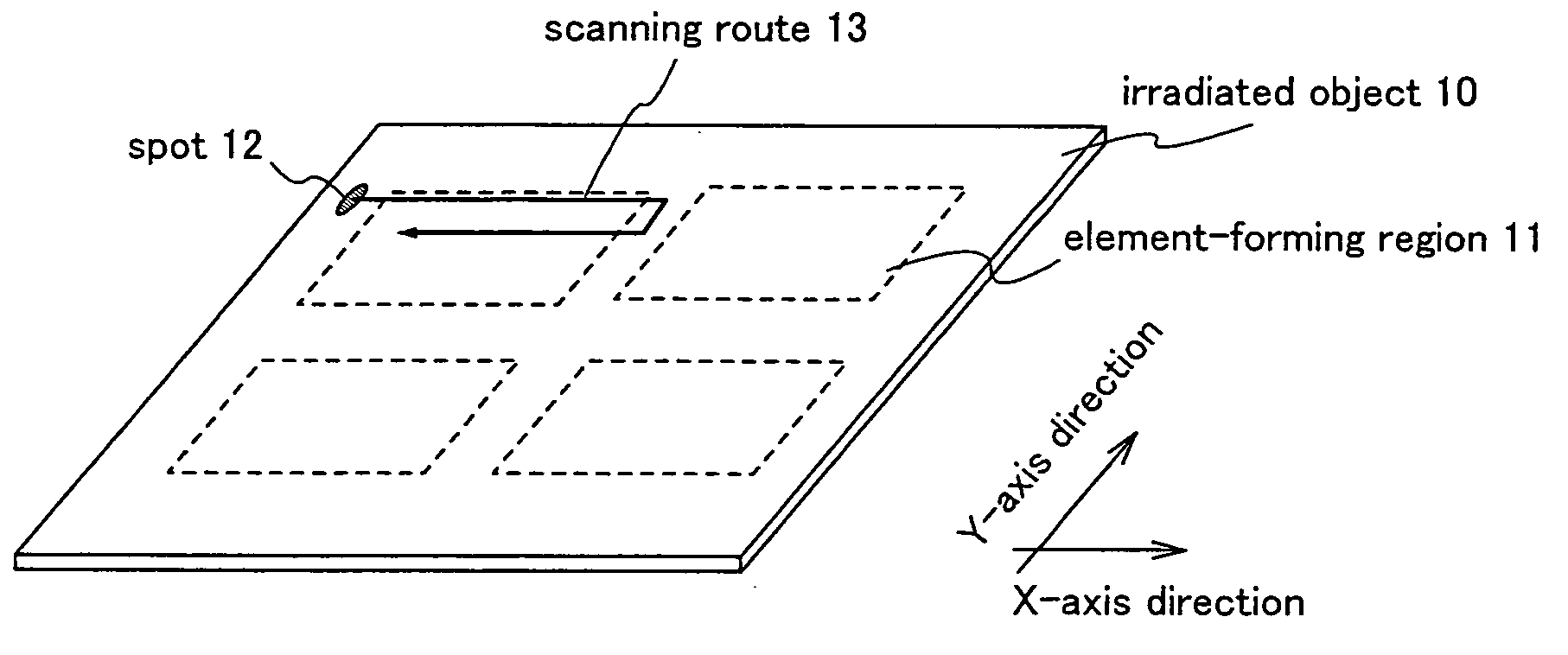
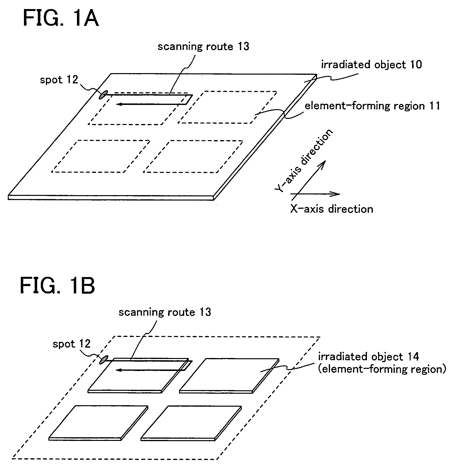
[0049] The present embodiment mode explains the case in which the laser processing is performed by employing the laser as the light source to the irradiated object in which four element-forming regions are formed.

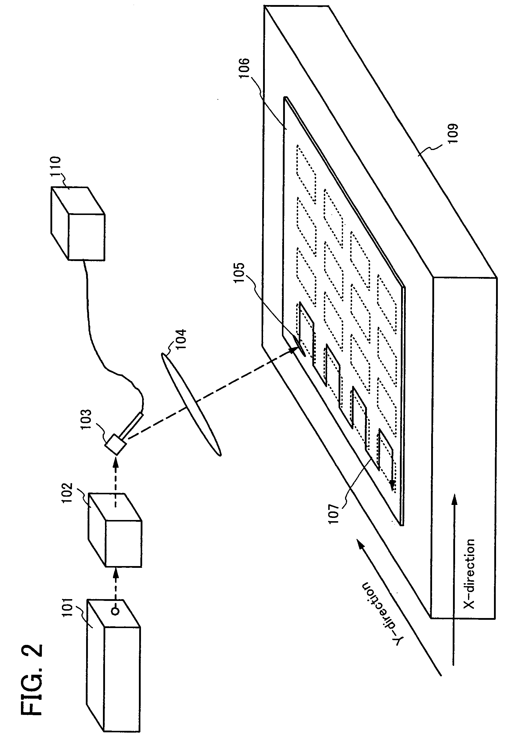
[0050] In a perspective diagram shown in FIG. 1(A), four of an element-forming regions 11 are provided in an irradiated object 10. And relative movements of the laser beam and the irradiated object move a spot 12 along a scanning route 13. The scanning route 13 is in XY directions where a major axis direction (X-axis direction in FIG. 1(A)) and a minor axis direction (Y-axis direction in FIG. 1(A)) are combined. On this occasion, for example, the first scanning means (for example, the galvanometer mirror or the polygon mirror) moves the spot in the major axis direction and the second scanning means (for example, an XY stage) moves the irradiated object in the minor axis direction. As thus described, the laser processing can be performed to the whole...


PUM

PropertyMeasurementUnit
aspect ratioaaaaaaaaaa
lengthaaaaaaaaaa

Abstract

The speed of the laser scanned by the scanning means such as a galvanometer mirror or a polygon mirror is not constant in the center portion and in the end portion of the scanning width. As a result, the object, for example an amorphous semiconductor film, is irradiated with the excessive energy and therefore there is a risk that the amorphous semiconductor film is peeled. In the present invention, in the case where the laser spot of the energy beam output continuously on the irradiated object is scanned by moving it back and forth with the use of the scanning means or the like, the beam is irradiated to the outside of the element-forming region when the scanning speed of the spot is not the predetermined value, for example when the speed is not constant, and accelerates, decelerates, or is zero, for example in the positions where the scanning direction changes, or where the scanning starts or ends.

Description

BACKGROUND OF THE INVENTION [0001] 1. Field of the Invention [0002] The present invention relates to a beam irradiation apparatus and a beam irradiation method. Moreover, the present invention relates to a method for manufacturing a thin film transistor using the apparatus and the method. [0003] 2. Description of Related Art [0004] A research has been conducted concerning a thin film transistor having a channel-forming region in a poly-crystalline semiconductor film (hereinafter this thin film transistor is referred to as poly-crystalline TFT) as a semiconductor element in a display device, an integrated circuit, or the like. With the development of the display device and the integrated circuit, further enhancement of the characteristic of the poly-crystalline TFT has been expected. [0005] Consequently, in order to enhance the characteristic of the poly-crystalline TFT, crystallization of the semiconductor film by a continuous wave laser irradiation apparatus has been examined. For ...

Claims


Application Information

Patent Timeline
Patent Type & Authority Applications(United States)
IPC IPC(8): B23K26/08H01L21/20H01L21/77H01L21/84
CPCB23K26/0807H01L27/1285H01L21/2026B23K26/0815B23K26/0821B23K26/082H01L21/02592H01L21/02683H01L21/02488H01L21/02422H01L21/0242H01L21/02425H01L21/02686H01L21/02678H01L21/02532H01L21/02595H01L21/02381H01L21/02691
Inventor YAMAZAKI, SHUNPEITANAKA, KOICHIROMIYAIRI, HIDEKAZU
Owner SEMICON ENERGY LAB CO LTD
Why Eureka
Try Eureka