Plasma display panel and process for producing the same and thin film

a technology of display panel and thin film, applied in the manufacture of electrodes, electrode systems, electric discharge tubes/lamps, etc., can solve the problems of low luminance, poor uv transmittance of film, and difficult fluoride film formation, etc., to reduce the degradation of luminance, reduce the amount of fluorine atoms, and reduce the effect of fluoride atom diffusion

Inactive Publication Date: 2005-02-24
PANASONIC CORP
View PDF1 Cites 18 Cited by
  • Summary
  • Abstract
  • Description
  • Claims
  • Application Information

AI Technical Summary

Benefits of technology

[0048] According to other aspect of the present invention, there is provided a thin film made of a fluoride selected from the group consisting of magnesium fluoride, calcium fluoride, barium fluoride and lithium fluoride, wherein the fluorine content in the thin film decreases in a direction from one surface of the film toward another surface of the film which is opposed the one surface. As similarly to the above, it is preferable that the fluorine content at or near the surface of the thin film is at a level of the fluorine content in a fluoride having a stoichiometric composition. This thin film is suitably used for covering a phosphor not only in a PDP but also in other light-emitting devices. When the thin film of the present invention is formed on a phosphor by using the phosphor as a base material, the coating can pass an amount of ultraviolet ray sufficiently while it can protect the phosphor from moisture, oxygen, plasma and so on, and the diffusion of fluorine atoms is suppressed since the film surface having the smaller fluorine content contacts with the phosphor. Therefore, it is possible to obtain a higher luminance, a smaller degradation in luminance and a smaller shift in a wavelength of a light emitted from the phosphor.
[0049] In another embodiment of the process of the present invention described above, the step for forming the coating is conducted by supplying fluorine into at least a part of a surface portion of the phosphor particle (more specifically into a surface portion of the phosphor particles or into a surface portion of the phosphor particles locating at the surface of the phosphor layer). As a result of supplying fluorine directly into the phosphor particle as above, a coating made of a fluorine-containing phosphor substance can be formed. It is possible to obtain a UV transmittance which is acceptable for properties of a PDP by appropriately setting a fluorine content in this coating. While the present invention is not bound by any theory, it is considered that the supplied fluorine atom occupies a hole as a crystal defect in a phosphor substance of the phosphor particle or substitutes an appropriate atom such as an oxygen atom in a crystal of the phosphor.

Problems solved by technology

In the prior art as described in the above, it is technically difficult and high cost to form the film of fluoride such as magnesium fluoride by a liquid phase method.
On the other hand, when the fluoride film is formed by a general gas phase method the present inventors have found problems in that the film has a poor UV transmittance thereof and thus a luminance is lowered contrary to the purpose of obtaining a higher luminance.
In addition, since the fluoride is hygroscopic, the fluoride is not necessarily a sufficient material for coating a phosphor particle.

Method used


Image

  • Plasma display panel and process for producing the same and thin film
  • Plasma display panel and process for producing the same and thin film
  • Plasma display panel and process for producing the same and thin film

Examples


first embodiment

[0088] First Embodiment

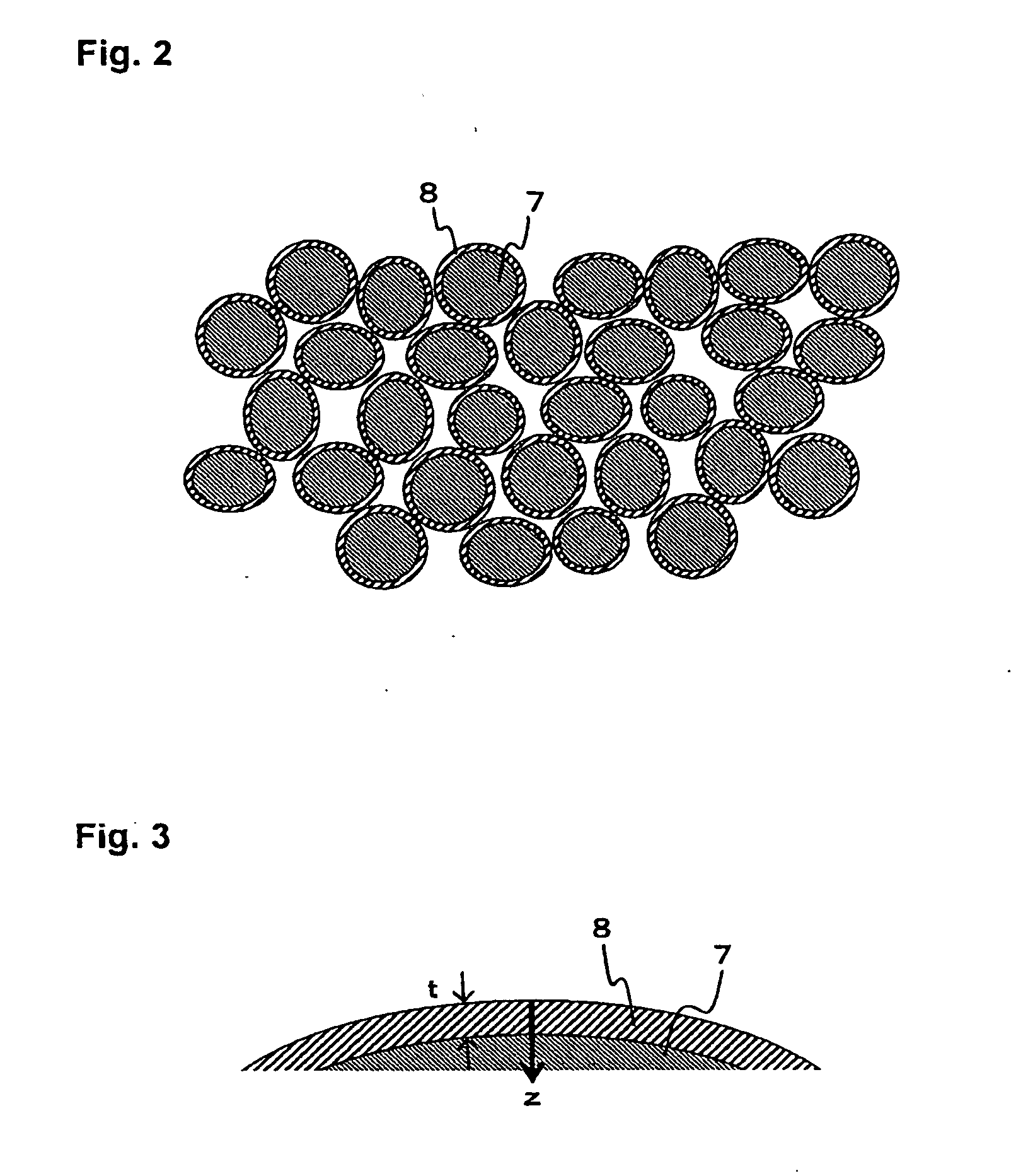
[0089] This embodiment relates to a PDP and a process for producing it in which the whole surface of each phosphor particle is covered with a coating made of a fluoride such as magnesium fluoride.

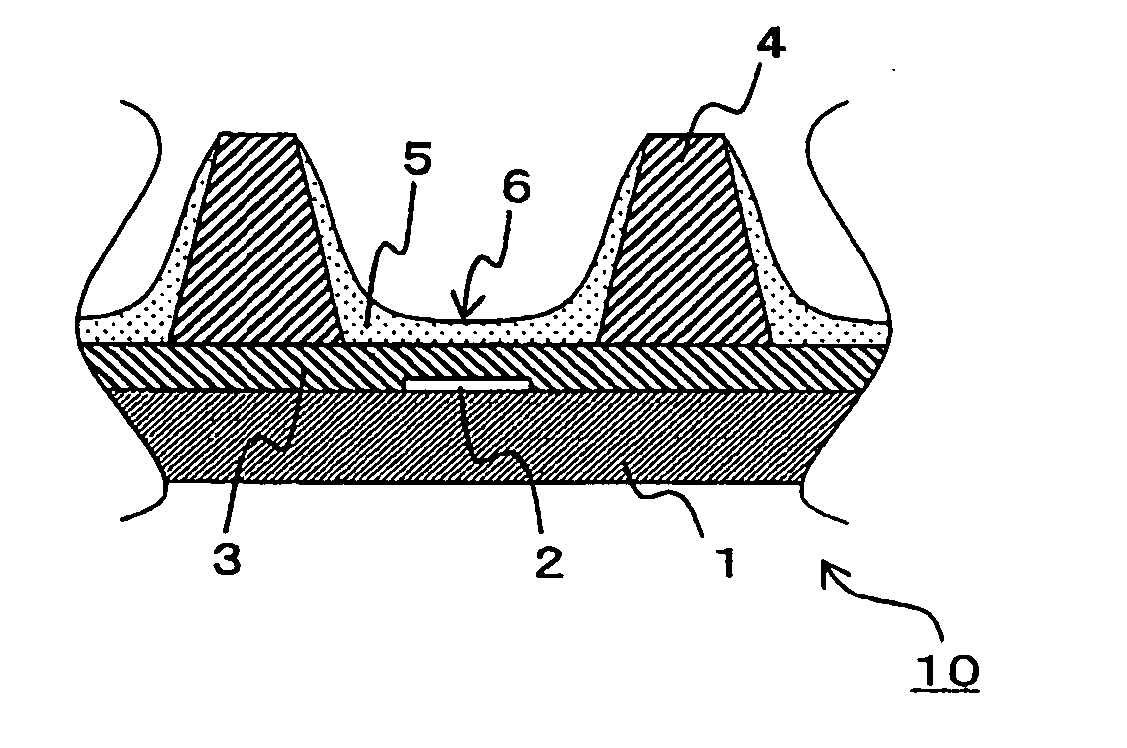
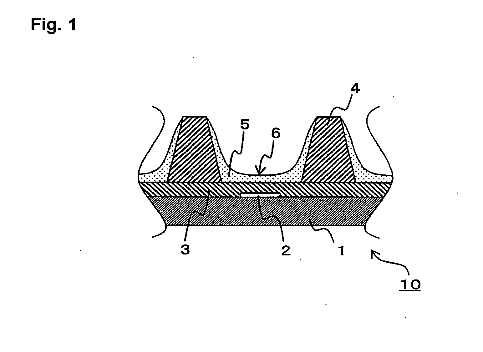
[0090] A PDP of the present embodiment is constructed by positioning a rear plate 10 shown in FIG. 1 to be opposed to a front plate (not shown) and form discharge spaces therebetween while locating a phosphor layer 6 inside, and by filling the discharge spaces with a discharge gas. In the rear plate 10, address electrodes 2 (one of which is shown in FIG. 1) are located on a rear substrate 1 which is generally made of glass, and a dielectric layer 3 covers the rear substrate 1 with the address electrodes 2. A plurality of ribs 4 is located on the dielectric layer 3 and each address electrode 2 is situated between the adjacent ribs 4. A phosphor layer 5 is formed between the adjacent ribs on a surface of the dielectric layer 3 covering the rear substrate 1 (as well as ...

second embodiment

[0118] Second Embodiment

[0119] This embodiment relates to a PDP and a process for producing it in which the whole surface of each phosphor particle is covered with a coating made of a fluoride-containing phosphor substance.

[0120] A PDP of the present embodiment may have a similar structure to that of the PDP of the first embodiment described above with reference to FIGS. 1 to 3, except for a material of a coating. A coating in the present embodiment is made of a fluoride-containing phosphor substance. In a case for a blue phosphor particle, for example, the coating includes atoms of fluorine, europium, barium, aluminum, magnesium and oxygen. In a case for a red phosphor particle, the coating includes atoms of fluorine, europium, yttrium and oxygen. In a case for a green phosphor particle, the coating includes atoms of fluorine, manganese, barium, aluminum and oxygen.

[0121] A thickness of the coating is preferably about 1 to 5 nm. A coating having a thickness less than 1 nm can not...

third embodiment

[0127] Third Embodiment

[0128] This embodiment relates to a PDP and a process for producing it in which the whole surface of each phosphor particle is covered with a coating made of a fluorine-added silicon oxide layer and a silicon oxide layer.

[0129] A PDP of the present embodiment may have a similar structure to that of the PDP of the first embodiment described above with reference to FIG. 1, except for a material and a structure of a coating. As shown in FIGS. 7 and 8, a coating in the present embodiment is made of a fluorine-added silicon oxide (SiOF) layer 11 and a silicon oxide (SiO2) layer 12 thereon.

[0130] A thickness of the fluorine-added silicon oxide layer 11 of the coating 8′ is preferably about 1 to 20 nm and more preferably about 1 to 15 nm. A thickness of the silicon oxide layer 12 of the coating 8′ is preferably about 1 to 10 nm and more preferably about 1 to 5 nm. With respect to both layers, a layer having a thickness less than 1 nm can not be formed with high rep...


PUM

PropertyMeasurementUnit
diameteraaaaaaaaaa
diameteraaaaaaaaaa
diameteraaaaaaaaaa

Abstract

A fluorine-containing precoating (not shown) is formed to cover a phosphor particle (7) by, for example, a physical vapor deposition of a fluoride. Then, a fluorine-containing coating (8) covering the phosphor particle (7) is formed by supplying fluorine into the precoating. Thus obtained phosphor particle (7) with the coating (8) is applied in the form of a paste to a substrate (1) on each electrode (2) is between adjacent two ribs (4) to form a phosphor layer (6) including the phosphor particles (7) between the ribs (4) on the substrate (1). The substrate (1) is positioned with respect to another substrate (not shown) having electrodes thereon to form discharge spaces between the substrates. The discharge spade is filled with a discharge gas to produce a plasma display panel (PDP).

Description

CROSS-REFERENCE TO RELATED APPLICATIONS [0001] The present application claims priorities under 35 U.S.C. §119 to Japanese Patent Application No. 2003-298481 filed on Aug. 22, 2003, entitled “PROCESS FOR PRODUCING PLASMA DISPLAY PANEL AND PLASMA DISPLAY PANEL AND THIN FILM” and Japanese Patent Application No. 2004-223717 filed on Jul. 30, 2004, entitled “PLASMA DISPLAY PANEL AND PROCESS FOR PRODUCING THE SAME AND THIN FILM.” The contents of these applications are incorporated herein by reference thereto in their entirety.BACKGROUND OF THE INVENTION [0002] 1. Field of the Invention [0003] The present invention relates to a plasma display panel (hereinafter referred to as PDP) which is used for displaying images on a television set, a computer or the like, and a process for producing such plasma display panel, and also a thin film which is preferably used for covering a phosphor (or fluorescent) substance. [0004] 2. Description of Related Art [0005] As generally known in the art, a PDP...

Claims


Application Information

Patent Timeline
Patent Type & Authority Applications(United States)
IPC IPC(8): C09K11/08C09K11/02C09K11/59C09K11/64C09K11/77H01J9/00H01J9/20H01J9/227H01J11/12H01J11/22H01J11/24H01J11/26H01J11/34H01J11/42
CPCC09K11/025H01J11/42H01J11/12C09K11/7734
Inventor OKUMURA, TOMOHIROSAITOH, MITSUOMORITA, MASASHIOKUMA, TAKAFUMITERAUCHI, MASAHARUASAYAMA, JUNKO
Owner PANASONIC CORP
Why Eureka
Try Eureka