Semiconductor integrated circuit device

a technology of integrated circuit device and semiconductor, which is applied in the direction of pulse technique, process and machine control, instruments, etc., can solve the problem that the step-down circuit cannot be installed in the semiconductor integrated circuit devi

Inactive Publication Date: 2005-02-24
RENESAS TECH CORP +1
View PDF6 Cites 8 Cited by
  • Summary
  • Abstract
  • Description
  • Claims
  • Application Information

AI Technical Summary

Benefits of technology

[0007] Further, a constant current source is used to cause a bias current for setting current consumption to flow in each differential amplifying MOSFET. A capacitor is provided between a circuit node responsive to a variation in external power supply voltage, and a ground potential to thereby detect a rise in the externa

Problems solved by technology

A problem arises in that current consumption allowed for the step-down circuit to realize such low power consumption results in about 120 nA

Method used


Image

  • Semiconductor integrated circuit device
  • Semiconductor integrated circuit device
  • Semiconductor integrated circuit device

Examples


Embodiment Construction

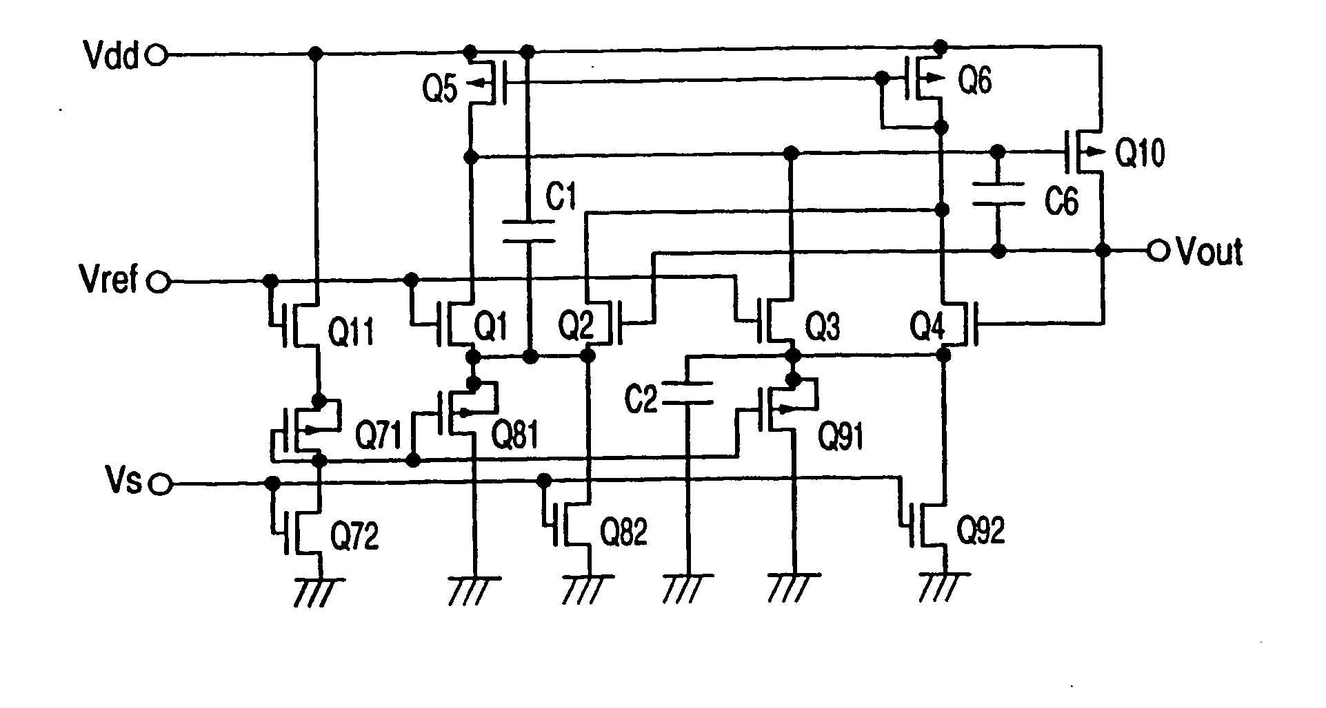
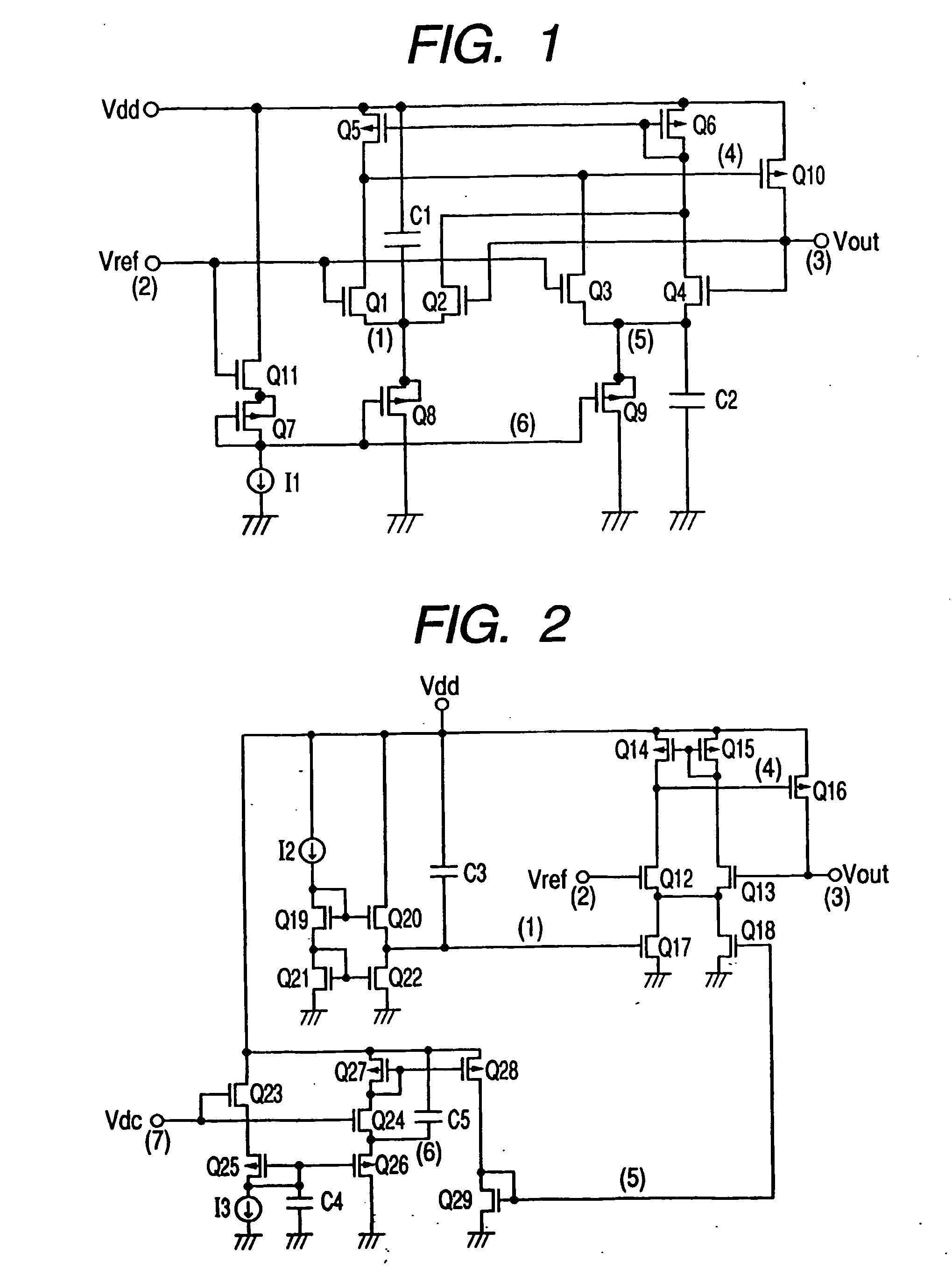
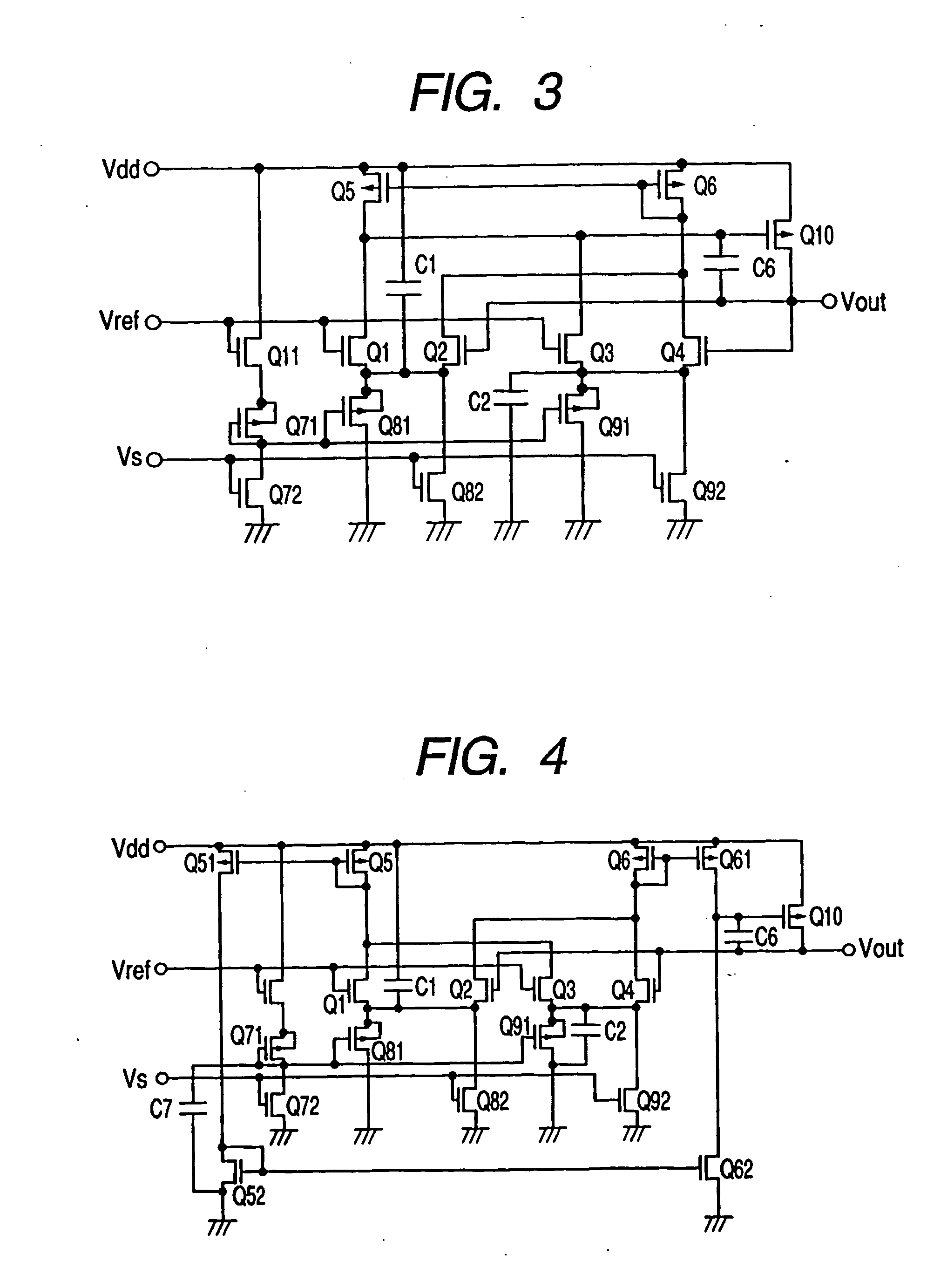
[0030] A circuit diagram of one embodiment of a negative feedback amplifier circuit installed in a semiconductor integrated circuit device according to the present invention is shown in FIG. 1. Respective circuit elements that constitute the present embodiment, are formed on a single substrate by the known CMOS semiconductor manufacturing technology together with other circuit elements that constitute the semiconductor integrated circuit device. The negative feedback amplifier circuit shown in the same drawing comprises a CMOS circuit made up of combinations of N-channel type MOSFETs and P-channel type MOSFETs. The P-channel type MOSFETs are distinguished from the N-channel type MOSFETs by marking their gates (channel portions) with arrows. This is similar even in the case of other circuit diagrams.

[0031] The negative feedback amplifier circuit according to the present embodiment constitutes a voltage follower circuit wherein its output voltage is fed back 100% to thereby power-amp...


PUM


Abstract

The present invention provides a semiconductor integrated circuit device equipped with a negative feedback amplifier circuit or a step-down circuit which realizes stabilization of an output voltage effectively in response to a variation in power supply voltage. A constant current source is used to cause a bias current for setting current consumption to flow in a differential amplifying MOSFET. A capacitor is provided between an external power supply voltage and a predetermined circuit node to thereby detect a reduction in the external power supply voltage. An operating current of the differential amplifying MOSFET is increased through the use of a current flowing in the capacitor due to such an external power variation, thereby executing the operation of stabilizing an output voltage corresponding to the reduction in the external power supply voltage.

Description

BACKGROUND OF THE INVENTION [0001] The present invention relates to a semiconductor integrated circuit device, and to, for example, a technology effective for application to one equipped with a step-down power circuit for stepping down an external power supply voltage and supplying it to an internal circuit. [0002] With advances in semiconductor processing technology, progress has been made toward reducing the size of each MOSFET and the size of a memory cell. Owing to the reduction in device size, a drop in operating voltage of the MOSFET has been performed in terms of problems such as a short channel effect and hot carriers, etc. On the other hand, an external supply source voltage of a semiconductor integrated circuit device is determined by a source or power supply voltage of a system equipped therewith. It is difficult to reduce such a system power supply voltage in association with the device size reduction that has been put forward in the semiconductor integrated circuit devi...

Claims


Application Information

Patent Timeline
IPC IPC(8): G05F1/56G11C11/413G05F1/565G11C5/14H01L21/822H01L27/04H03F1/30H03F3/45H03K19/00
CPCG05F1/56G05F1/565G11C5/147H03F2203/45458H03F3/345H03F3/45179H03F2200/513H03F1/34G11C5/14
Inventor SAITOH, YOSHIKAZU
Owner RENESAS TECH CORP
Why Eureka
Try Eureka