Generating sets of tailored laser pulses

a laser pulse and laser pulse technology, applied in multiplex communication, manufacturing tools, semiconductor/solid-state device details, etc., can solve the problems of complicated link severing process, reduced processing quality, and difficult to completely remove such links with a single pulse of conventional laser output at sufficient throughput without causing unacceptable damage to surrounding materials, so as to improve the processing quality of removal

Active Publication Date: 2005-02-24
ELECTRO SCI IND INC
View PDF17 Cites 71 Cited by
  • Summary
  • Abstract
  • Description
  • Claims
  • Application Information

AI Technical Summary

Benefits of technology

[0014] An object of the present invention is to provide a method of and an apparatus for improving the processing quality of removal of conductive link material and overlying passivation structure material fabricated on a substrate.

Problems solved by technology

One current trend in link manufacturing is to make relatively thick links (greater than about 1 μm thick to about 2 μm thick or thicker) from metallic materials, and such links complicate the link severing process even further.
It has proven particularly difficult to completely remove such links with a single pulse of conventional laser output at sufficient throughput without causing unacceptable damage to surrounding materials.
Unfortunately, this practice would entail either a long dwell time over each link or separate duplicative scanning passes of repositioning and refiring at each selected link, effectively reducing the throughput by factor of about two or more.

Method used


Image

  • Generating sets of tailored laser pulses
  • Generating sets of tailored laser pulses
  • Generating sets of tailored laser pulses

Examples


Embodiment Construction

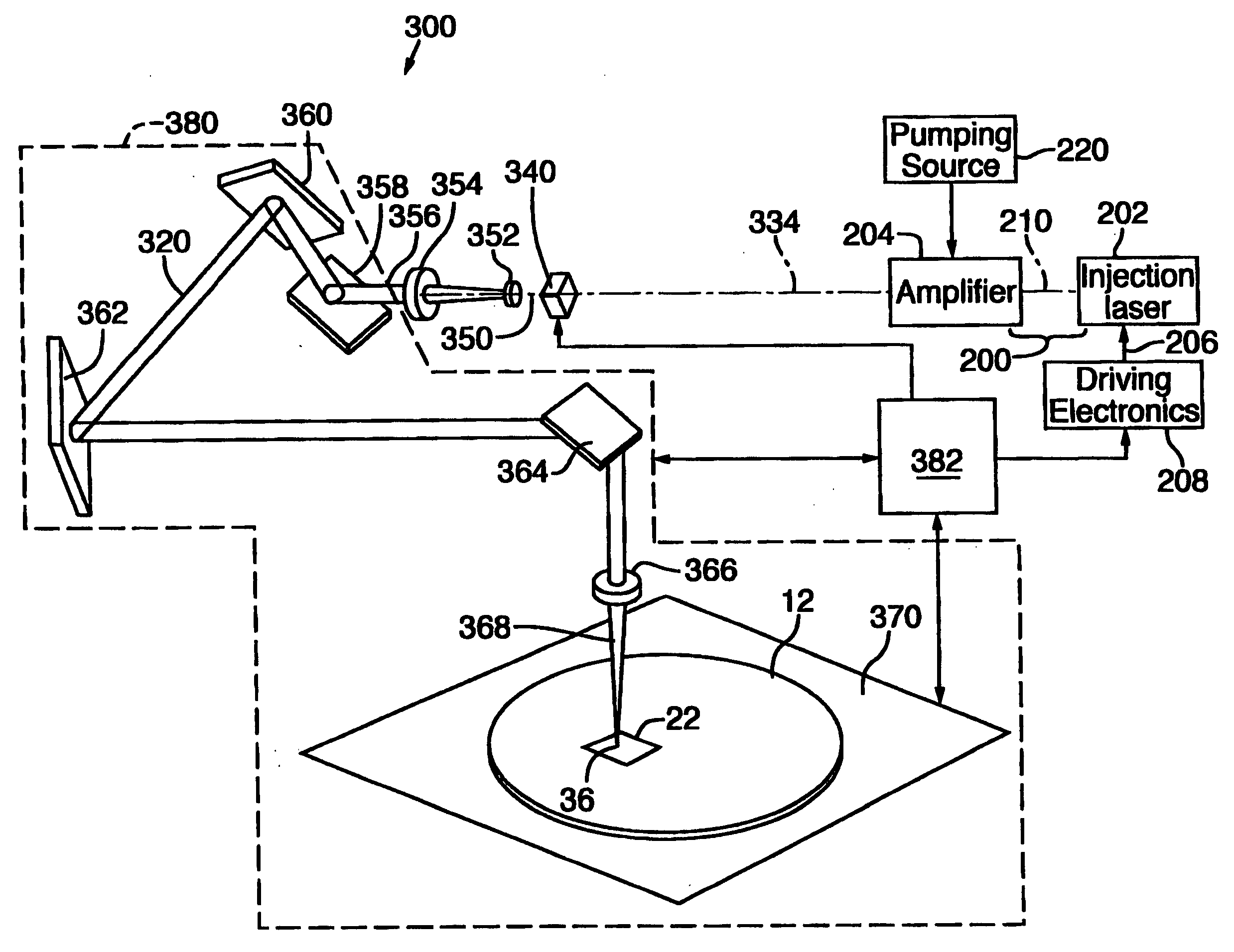
[0045]FIG. 6A is a partly schematic, simplified diagram of an embodiment of an exemplary laser system 300 implemented with a MOPA laser 200 and a beam delivery and material positioning system 380 (positioning system 380) that cooperate with a laser processing control system to process links 22. With reference to FIG. 6A, a MOPA laser 200 includes an injection laser 202 followed by an amplifier 204. Injection laser 202 can be a diode laser having a fast response time and delivering laser output 210 at a laser wavelength that matches the gain spectrum of amplifier 204. Such a diode laser can be a single frequency laser employing integrated distributed feedback or a distributed Bragg reflector, or such diode laser can be tuned with extracavity components. Such a diode laser can also be a multimode diode laser.

[0046] Amplifier 204 is preferably a fiber amplifier comprising a conventional fiber lasant material and is preferably pumped by a conventional continuous wave (CW) pumping sourc...


PUM

PropertyMeasurementUnit
rise timeaaaaaaaaaa
rise timeaaaaaaaaaa
laser energyaaaaaaaaaa

Abstract

In a master oscillator power amplifier, a driver (208) of a diode laser (202) is specially controlled to generate a set of two or more injection laser pulses that are injected into a power amplifier (204) operated in an unsaturated state to generate a set (50) of laser pulses (52) that replicate the temporal power profile of the injection laser pulses to remove a conductive link (22) and/or its overlying passivation layer (44) in a memory or other IC chip. Each set (50) includes at least one specially tailored pulse (52) and/or two or more pulses (50) having different temporal power profiles. The duration of the set (50) is short enough to be treated as a single “pulse” by conventional positioning systems (380) to perform on-the-fly link removal without stopping.

Description

RELATED APPLICATIONS [0001] This patent application claims benefit of U.S. Provisional Application No. 60 / 496,631, filed Aug. 19, 2003.COPYRIGHT NOTICE [0002]© 2004 Electro Scientific Industries, Inc. A portion of the disclosure of this patent document contains material which is subject to copyright protection. The copyright owner has no objection to the facsimile reproduction by anyone of the patent document or the patent disclosure, as it appears in the Patent and Trademark Office patent file or records, but otherwise reserves all copyright rights whatsoever. 37 CFR § 1.71(d). TECHNICAL FIELD [0003] The present invention relates to laser processing of conductive links on memory chips or other integrated circuit (IC) chips and, in particular, to methods and systems employing a master oscillator power amplifier to generate sets of at least two laser pulses to sever such links with better processing quality on-the-fly. BACKGROUND OF THE INVENTION [0004] Decreased yields in IC device ...

Claims


Application Information

Patent Timeline
Patent Type & Authority Applications(United States)
IPC IPC(8): B23KB23K26/06B23K26/38H01SH04J14/02
CPCB23K26/0613B23K26/063B23K2201/40H01L23/5258H01L2924/0002H01L2924/00B23K26/0622B23K2101/40B23K26/00H01S3/10007H01S3/101B23K26/0608
Inventor SUN, YUNLONGHAINSEY, ROBERT F.
Owner ELECTRO SCI IND INC
Why Eureka
Try Eureka