Image displaying method and image displaying device

a technology of image display and image, applied in the direction of digital storage, radio frequency controlled devices, instruments, etc., can solve the problems of numerous problems, thin-film diodes have difficulty in gaining the required on/off ratio, and the memory cell structure is disclosed, so as to reduce the size of the process, reduce the cell area, and stable cell operation

Inactive Publication Date: 2005-02-24
IBM CORP
View PDF6 Cites 23 Cited by
  • Summary
  • Abstract
  • Description
  • Claims
  • Application Information

AI Technical Summary

Benefits of technology

[0012] Each of the foregoing junction diodes is formed either on the SOI substrate or on the insulating film on the semiconductor substrate. Accordingly, the diode is isolated from the substrate and thereby does not generate a parasitic transistor. In this way, it is possible to achieve stable cell operations regardless of application modes of bias voltages when the MRAM is operating. Moreover, since the adopted switching element is not an FET but is a diode, it is possible to reduce a cell area. Such a switching element is advantageous to downsizing process.
[0013] Here, plane patterns of the p-type and the n-type impurity diffused regions constituting the junction diode can be either formed into mutually symmetrical shapes or formed in a manner that one of the impurity diffused regions surrounds the other impurity diffused region. In the latter case, it is possible to secure a larger area for junction, whereby on-state resistance of the diode can be reduced. Moreover, the p-type impurity diffused region and / or the n-type impurity diffused region can be formed continuously and integrally in the direction of a word line(s). In this case, standard electric potential of each memory cell can be made constant, and stable memory cell operations are thereby expected.
[0014] Moreover, when the diode is made of the semiconductor layer such as a polycrystalline silicon film, the semiconductor layer can be formed simultaneously with formation of a gate electrode of an FET in a logic circuit such as a peripheral circuit. When the diode is formed by diffusion of the impurity on the surface layer of the SOI substrate surface layer, the diode can be formed simultaneously with formation of a source or a drain electrode of a transistor in the logic circuit such as a peripheral circuit. In this way, the diode can be formed in the same steps as the steps of diffusing impurities and of forming the gate electrode in the process of forming the logic circuit. Accordingly, there are very few additional steps upon formation of the junction diode of the present invention. In other words, a fabricating method proposed by the present invention can be regarded as a process excellent in compatibility with the fabricating process of the logic circuit or the like.

Problems solved by technology

Nevertheless, the memory cell structure disclosed in Document 1 involves numerous problems.
Firstly, the thin-film diode has difficulty in gaining a required on / off ratio.
Whereas an on / off ratio of about four digits is preferred, the current thin-film diode cannot gain such an on / off performance easily.
Secondly, there is a problem of flatness of a substrate required in the MTJ element.
Nevertheless, it is difficult for the thin-film diode to achieve such atomic-level flatness, because the thin-film diode is generally made of a polycrystalline silicon film.
Accordingly, it is extremely difficult to stack the MTJ element having a predetermined characteristic onto the thin-film diode.
Thirdly, on-state resistance of the thin-film diode incurs a problem along with downsizing of the MTJ element.
Although there is growing possibility for downsizing the MTJ element in line with characteristic improvements thereof, it is not possible to reduce the on-state resistance of the thin-film diode relevantly to such a downsizing level.
Due to existence of the foregoing disadvantages, it is currently conceived difficult to realize the memory cell structure of stacking the MTJ element on the thin-film diode.
Furthermore, since the MTJ element is formed on an insulating film and on a metallic film where sufficient flatness can be secured, disadvantages as cited in the case of the thin-film diode do not exist therein.
Nevertheless, the memory cell disclosed in Document 2 also involves the following problems.
Depending on aspects of biasing the memory cell, there may be a case where the parasitic transistor starts functioning and a memory cell operation cannot be secured as intended at a designing stage.
However, the memory cell composed of the gated diode and the MTJ element cannot fulfill a small occupied area.
Therefore, the memory cell is disadvantageous to downsizing.

Method used


Image

  • Image displaying method and image displaying device
  • Image displaying method and image displaying device
  • Image displaying method and image displaying device

Examples


first embodiment

[0065] (First Embodiment)

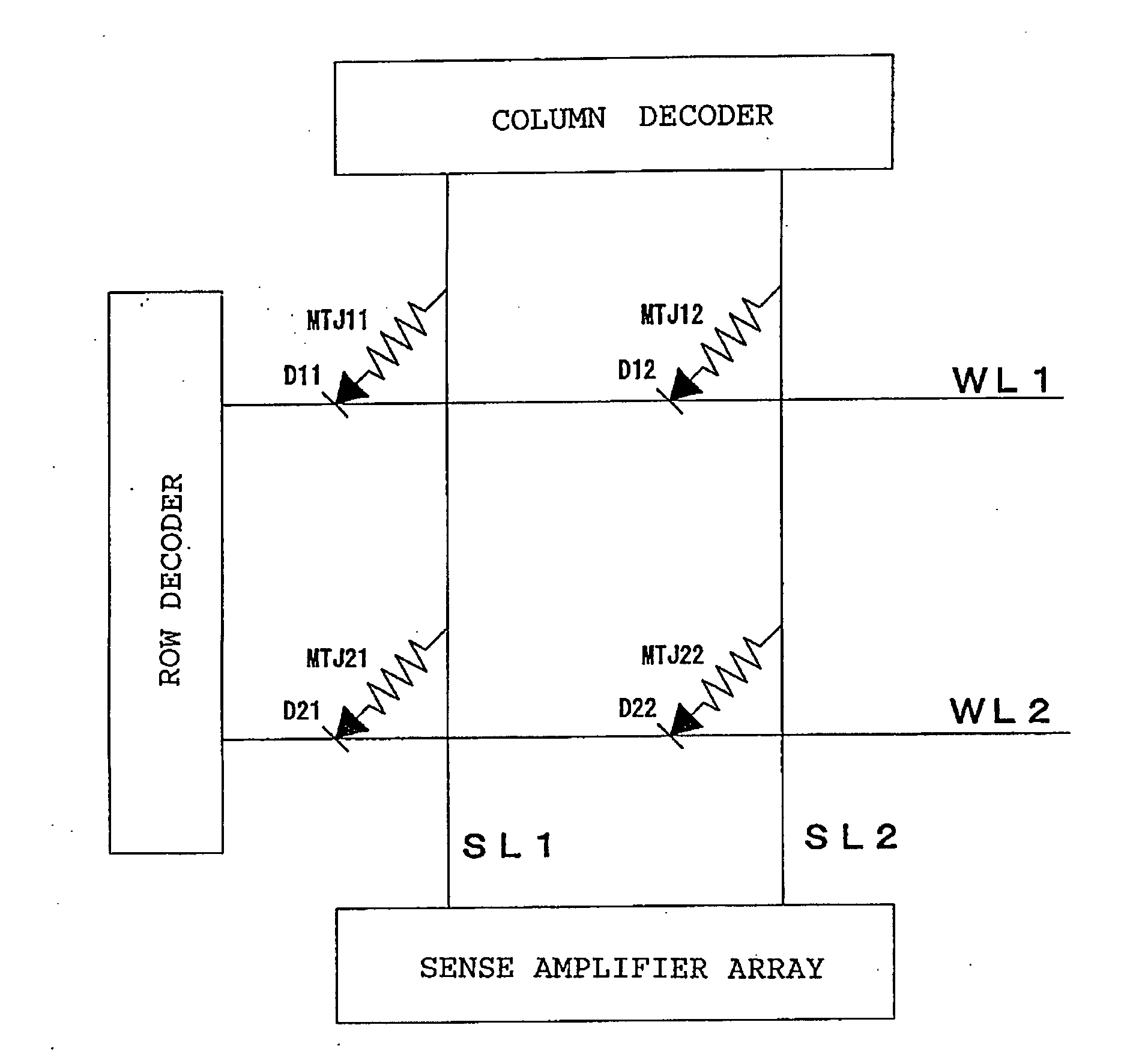
[0066]FIG. 1 is a circuit diagram showing one example of a memory device (an MRAM) of an embodiment of the present invention, which illustrates partially regarding a memory cell region in particular. As shown in FIG. 1, the MRAM of this embodiment includes word lines WL and sense lines SL. Moreover, magnetic tunnel junction elements MTJ and diodes D are disposed on respective intersecting points of the word line WL and the sense line SL. The magnetic junction element MTJ and the diode D are connected serially to constitute a memory cell. One end (an MTJ end) of the memory cell is connected to the sense line SL and the other end (a D end) thereof is connected to the word line WL. Selection of a memory cell is conducted by selecting one of the sense lines SL and one of the word lines WL, whereby the memory cell located at an intersecting point of the selected sense line SL and the selected word line WL becomes a selected memory cell. Selection of the sense lin...

second embodiment

[0115] (Second Embodiment)

[0116] An MRAM according to this embodiment is an example of modifying structures of the diodes in the MRAM described in first embodiment. In the following, description regarding the same constitutions as those in first embodiment will be omitted, whereby description will be highlighted on different parts from first embodiment.

[0117]FIG. 24 shows a cross-sectional view and a plan view partially exemplifying a memory cell array and a peripheral circuit on one example of an MRAM according to the second embodiment. The MRAM of this embodiment is formed on a silicon substrate (a silicon wafer) 50. An isolation region 53 is formed on a surface portion of the silicon substrate 50, and a p well 54 and an n well 55 to be defined by the isolation region 53 are formed in a peripheral circuit region. An n-channel-type MOSFET is formed on the p well 54 and a p-channel-type MOSFET is formed on the n well 55. Diodes are formed on the isolation region 53 in a memory cell...

third embodiment

[0128] (Third Embodiment)

[0129] An MRAM according to this embodiment is an example of further modifying structures of the diodes in the MRAM described in first embodiment. In the following, description regarding the same constitutions as those in first embodiment will be omitted, whereby description will be highlighted on different parts from first embodiment.

[0130]FIG. 36 shows a cross-sectional view and a plan view partially exemplifying a memory cell array and a peripheral circuit on one example of an MRAM according to the third embodiment. The MRAM of this embodiment is formed on an SOI substrate as similar to the first embodiment. However, the diode of the third embodiment is different from the diode of the first embodiment in that the diode of the third embodiment includes an n-type semiconductor layer 71 generated from a surface semiconductor layer 3 of the SOI substrate, and a p-type semiconductor layer 75 patterned simultaneously with formation of gate electrodes of MOSFET...


PUM


Abstract

Provided is an MRAM memory cell structure capable of preventing generation of parasitic transistors. Diodes are adopted as switching elements of an MRAM memory cell. An n-type semiconductor layer and a p-type semiconductor layer, which collectively constitute a diode, are formed on a surface semiconductor layer of an SOI substrate. The n-type semiconductor layer and the p-type semiconductor layer are disposed in a lateral direction and isolated by an isolation region, whereby the diode is isolated electrically from other elements and from the substrate.

Description

TECHNICAL FIELD [0001] The present invention relates to nonvolatile memory devices. More specifically, the present invention relates to technologies to be applied effectively to a memory device adopting a spin valve which utilizes magnetoresistive effects such as a tunnel magnetoresistive effect. BACKGROUND [0002] A random access memory (RAM) utilizing a magnetoresistive effect, in which a resistance value varies depending on a magnetic orientation, is drawing attention recently. Such a RAM utilizing the magnetoresistive effect is referred to as a magnetoresistive RAM (MRAM). Magnetoresistive effects includes an anisotropic magnetoresistive (AMR) effect, a giant magnetoresistive (GMR) effect, and the like are known. In particular, a tunnel magnetoresistive (TMR) effect, which gains a magnetoresistive effect by use of a tunneling current, is highlighted for capability of gaining large magnetic-field sensitivity. [0003] A spin-valve element using the TMR has a laminated structure incl...

Claims


Application Information

Patent Timeline
Patent Type & Authority Applications(United States)
IPC IPC(8): G11C11/15G11C11/36H01L21/336H01L21/84H01L27/10H01L27/105H01L27/146H01L27/22
CPCH01L27/224H01L21/84H10B61/10G11C11/15
Inventor KITAMURA, KOHJISUNAGA, TOSHIOMIYATAKE, HISATADA
Owner IBM CORP
Why Eureka
Try Eureka